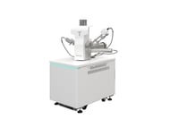
Interview | Why Tescan VEGA™ Remains a Practical SEM for Materials R&D and Quality Control
Discover how Tescan VEGA™ supports materials characterization, SEM-EDS analysis, industrial quality control and failure analysis.
Read more
Scientific insights, technical resources and expert knowledge to help you get more from your research.
Discover how Tescan VEGA™ supports materials characterization, SEM-EDS analysis, industrial quality control and failure analysis.
Read more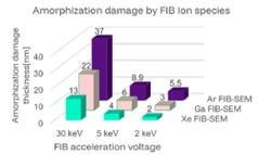
Download the application note to compare Ga⁺, Xe⁺ and Ar⁺ ion milling for low-damage TEM sample preparation and improved lamella quality.
Read more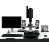
See how Tescan EXLO enables fast ex-situ TEM lift-out, with novice users achieving specimen transfers in under three minutes at M&M 2026.
Read more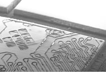
See how CT, laser delayering and SEM reveal buried structures in advanced semiconductor packages while preserving spatial context.
Read more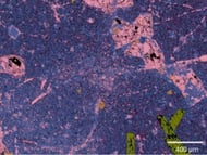
Discover how TIMA™ Geolite supports automated mineralogy, mineral identification and efficient analysis workflows for research samples.
Read more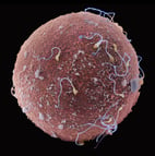
Explore how SEM, FIB-SEM, volume EM and cryo-EM reveal biological structures from surface morphology to cells, organelles and molecular detail.
Read more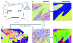
Download the application note to explore automated high-temperature in situ EBSD for tracking phase evolution and grain refinement in AM steel.
Read more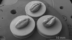
Explore the science of beer, from malting and hops to yeast fermentation, filtration and foam, revealed through electron microscopy.
Read more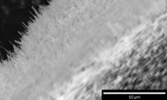
Download the application note on correlative cryo-EM and cryo-ET sample preparation for imaging bacteria–biomaterial interfaces.
Read more
Explore Tescan highlights from IMC21 in Liverpool, including SEM, FIB-SEM, 4D-STEM, micro-CT, live demos and scientific presentations.
Read more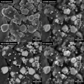
Learn how SEM detectors use SE and BSE signals, angular filtering and energy filtering to control contrast and reveal material information.
Read more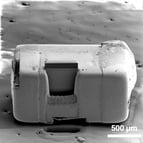
Learn how multiscale imaging and electron microscopy improve materials characterization by revealing details from the macro to nanoscale.
Read more
See how Tescan CLARA™ SEM imaging reveals microstructural changes in cork stoppers after thermal aging in water and ethanol.
Read more
Learn how ultra-high-resolution SEM enables nanoscale imaging, low-voltage analysis and advanced materials characterization with Tescan MIRA XR.
Read more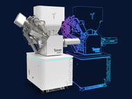
Explore how digital twin technology can support electron microscopy workflows, instrument understanding, training, and operational efficiency.
Read more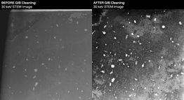
Learn how argon ion polishing reduces gallium-induced damage and improves TEM lamella quality for reliable high-resolution analysis.
Read more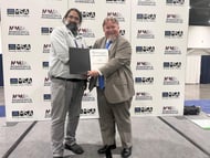
Tescan FemtoChisel™ receives the Microscopy Innovation Award 2026 for advancing fast, precise femtosecond laser sample preparation.
Read more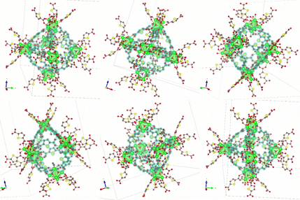
Discover the new Cryo-EM solution for Tescan TENSOR™ with low-dose Cryo-STEM, Cryo-EDS, Cryo-4D STEM and Cryo-3D ED workflows.
Read more
Watch the on-demand webinar to explore cryo-STEM, cryo-EDS, cryo-4D-STEM and cryo-3D ED workflows for beam-sensitive materials using Tescan TENSOR™.
Read more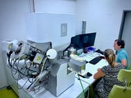
Explore cryo-FIB-SEM, cryo lift-out and correlative microscopy workflows for targeting and preparing beam-sensitive biological samples.
Read more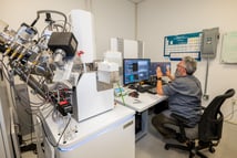
Discover how Tescan AMBER™ X supports diverse research workflows in an open-access microscopy facility using plasma FIB-SEM.
Read more
Discover how Dr. Kati Valtonen uses Tescan CLARA™ for wear research, materials characterization, EBSD, and in situ SEM analysis.
Read more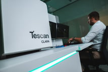
Discover the new Tescan CLARA™ Ultra-High-Resolution SEM with advanced SEM contrast for deeper materials characterization and nanoscale imaging.
Read more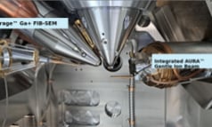
Download the application note to learn how Ar⁺ ion beam polishing reduces Ga⁺ FIB artifacts for reliable TEM sample preparation.
Read more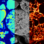
Learn what FIB-SEM is, how it works, and why it is essential for nanoscale imaging, sample preparation, and advanced materials characterization.
Read more
Tescan launches the new CLARA™, an ultra-high-resolution SEM designed for nanoscale materials characterization and advanced imaging.
Read more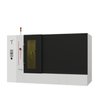
Discover how non-destructive micro-CT imaging revealed new insights into the 2,400-year-old Tollund Man and archaeological research.
Read more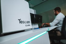
Watch the Tescan CLARA™ webinar on demand and explore ultra-high-resolution SEM imaging, advanced contrast, intelligent detection, and automated workflows.
Read more
Discover how Micro-CT revealed the internal condition of a baseball bat after 2,000 swings using non-destructive 3D X-ray imaging.
Read more
Discover how Tescan grew from a small team in Brno into a global leader in electron microscopy and scientific instrumentation.
Read more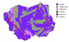
Discover how Tescan TIMA™ automated mineralogy helped researchers analyze Chang'e-6 lunar samples and refine our understanding of the Moon.
Read moreWatch how baseplate heating, build height and carbide networks influence cracking, porosity and microstructure in LPBF-processed PM23 high-speed steel.
Read more
Tescan joins the Shimadzu Group, expanding innovation, global reach, and integrated solutions while maintaining its customer-focused approach.
Read more
Learn how 4D micro-CT reveals freeze-drying dynamics and helps researchers study structural changes non-destructively.
Read more
Discover how integrated argon polishing improves TEM lamella preparation, repeatability, and FIB-SEM specimen quality.
Read more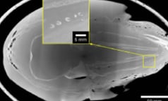
Download the application note to discover high-resolution micro-CT imaging of a baleen whale fetus for museum and anatomy research.
Read more
Download the application note to explore dynamic micro-CT imaging of dough rising, pore formation, and bread baking in real time.
Read more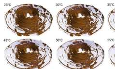
Download the application note to explore dynamic micro-CT imaging of Li-ion battery heating, electrolyte movement, and gas formation.
Read more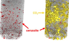
Discover how Tescan Spectral CT enables real-time 4D analysis of metal leaching, elemental quantification, and hydrometallurgical processes.
Read more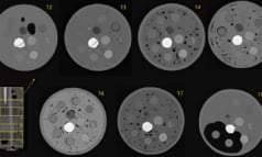
Learn how Tescan SPECTRAL CT with True Contrast enables accurate identification and analysis of multi-polymer composites using spectral micro-CT imaging.
Read more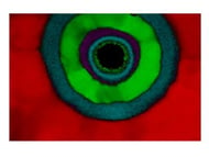
An interview with Stanislav Haviar on 4D-STEM in SEM, thin-film materials research, and how Tescan AMBER 2 supports advanced characterization workflows.
Read more
Tescan announces the winner of the UniTOM® XL Dynamic CT Beam Time Competition 2026 and the selected carbonate dissolution research project.
Read more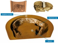
Learn how researchers at TUM use micro-CT to study food drying, plant-based foods, root-soil interactions, and dynamic processes.
Read more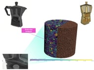
Learn how micro-CT enables non-destructive 3D and 4D imaging, helping researchers visualize internal structures and dynamic processes.
Read more
Learn why FIB-SEM is the preferred method for TEM specimen preparation, enabling site-specific targeting, faster workflows, and reliable results.
Read more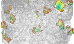
Visualize cooling-induced crystallization in porous materials with Tescan UniTOM HR. Capture crystal growth, dissolution, and pore-scale changes in real time.
Read more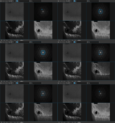
Watch the on-demand webinar to learn how event-based 4D-STEM in SEM improves sample screening, diffraction analysis, and TEM workflow efficiency.
Read more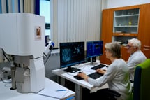
Discover how researchers at the University of Žilina use electron microscopy and Tescan MIRA XR to study metallic materials, fractography, structural changes, and industrial failures
Read more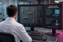
Learn how a scanning electron microscope (SEM) works using the simple analogy of the Battleship game. Explore SEM signals, raster scanning, and FIB-SEM workflows.
Read more
Discover how Tescan’s integrated retractable 4D-STEM detector enables diffraction-based analysis directly in SEM and FIB-SEM workflows for advanced materials characterization.
Read more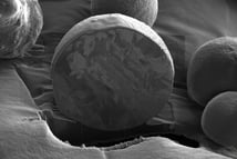
Discover how Micro-CT, ultrafast laser processing, and FIB-SEM create a faster, more reliable failure analysis workflow for advanced semiconductor packaging.
Read more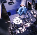
Learn the fundamentals of sample preparation in electron microscopy, including cleaning, coating, mounting, TEM lamella preparation, and cryo-EM workflows.
Read more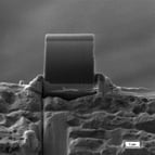
Learn how TEM lamella thickness and window width influence stability during FIB preparation. Practical guidance for reducing bending, uneven polishing, and punch-through risk.
Read more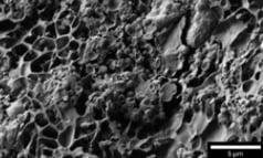
Download App Note and discover how cryogenic SEM enables high-resolution imaging of dairy microstructure, preserving native morphology to support formulation, processing, and food research.
Read more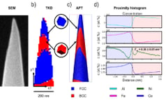
Accelerate APT specimen preparation with Tescan AMBER X 2. Combine fast Xe plasma FIB milling with high-precision site-specific targeting for high-quality atom probe tomography workflows.
Read more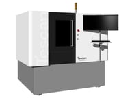
Discover how FemtoChisel™ laser solutions enable precise and efficient sample preparation workflows, supporting advanced microscopy and materials analysis.
Read more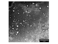
Learn how integrating low-energy argon ion beam cleaning with Ga+ FIB-SEM improves (S)TEM sample preparation by reducing damage and enabling high-quality nanoscale analysis.
Read more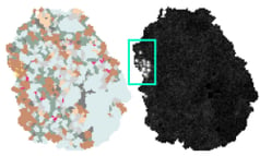
Optimize gold recovery with TIMA automated mineralogy. Analyze grain size, mineral associations, and refractory gold for better geometallurgical decisions.
Read more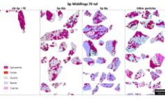
Analyze ore texture and mineral liberation with Tescan TIMA™. Gain quantitative insights for grind optimization, flowsheet design, and ore processing.
Read more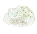
Learn the fundamentals of electron microscopy, including how SEM, TEM, and STEM work, how images are formed, and what signals reveal about materials at the nanoscale.
Read more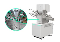
Watch the on-demand webinar on TEM lamella preparation using AMBER 2 and Aura™ Gentle Ion Beam to improve sample quality, reproducibility, and throughput.
Read more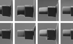
Improve lab efficiency with automated TEM sample preparation using Orage 2 Ga+ FIB. Achieve consistent lamella quality and faster workflows.
Read more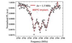
Download the application note to discover how high-temperature ion implantation increases diamond NV center density and improves photoluminescence.
Read more
An interview on CEITEC Nano infrastructure, plasma FIB-SEM with SIMS, and advanced materials workflows using Tescan AMBER X 2.
Read more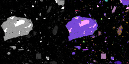
Watch the on-demand webinar on correlated particle analysis workflows using TIMA, FIB-SEM and SIMS for advanced microanalysis and isotopic characterization.
Read more
Explore how Tescan TIMA™ enables automated mineral mapping and phase identification in geological samples from Kerguelen Island using advanced mineralogy workflows.
Read more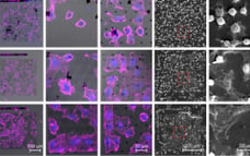
Discover how electron beam lithography enables precise nanopatterning of biomolecules to control cell behavior, receptor interactions, and nanoscale signaling in life sciences research.
Read more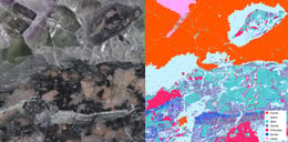
Learn how automated mineralogy and Tescan TIMA help mining teams make faster, decision-ready processing choices. Insights from mineralogist Braam Smit.
Read more
Explore how in-situ micro-CT enables non-destructive 3D analysis of thermally induced displacements in semiconductor packaging, improving reliability and failure analysis.
Read more
Download the application note to explore how SEM identifies plant species through leaf surface morphology and large-area imaging.
Read more
Download the application note to explore AMBER X FIB-SEM for precise sub-20nm node delayering and in-situ nanoprobing while preserving electrical properties.
Read more
Discover how micro-CT supports embryology and fetal imaging in clinical environments. Insights from Bernadette de Bakker on 3D imaging, research, and care.
Read more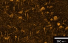
Download application note showing how Tescan TENSOR enables multimodal 4D-STEM and EDX analysis of AA2099 Al–Li alloy to map precipitates and microstructure.
Read more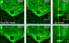
Download the application note to learn how fluorescence-guided cryo-FIB prepares intracellular protein crystals for high-resolution TEM imaging and diffraction.
Read more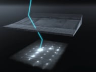
Learn what STEM is, how it works and how it compares to TEM. Explore 4D-STEM, electron diffraction and analytical techniques for materials and semiconductors.
Read more
Tescan offers on‑site demos in a new scanning electron microscopy lab in Korea, supporting the semiconductor industry, research institutions and universities with FIB‑SEM expertise.
Read more
The INDICO FEBID workshop in Frankfurt advanced digital control for reliable 3D nanoprinting. Tescan contributed expertise in SEM-based nanofabrication, FIBID and in situ process monitoring.
Read more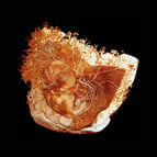
Discover how micro-CT imaging is transforming prenatal care and early human development research through non-destructive, high-resolution 3D anatomical analysis.
Read more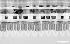
Application note on automated Ga⁺ FIB-SEM TEM lamella preparation for high-throughput, reproducible multimodal STEM analysis of 3nm FinFET devices.
Read more
Watch this on-demand webinar on improving TEM specimen preparation with Tescan AMBER 2 Ga⁺ FIB-SEM, Orage 2, automation, and integrated gentle ion beam polishing for advanced materials characterization.
Read more
Register for the FemtoChisel™ webinar to explore ultrafast laser processing, semiconductor sample preparation and a live product demonstration.
Read more
Watch Tescan’s webinar on tailored cryo-EM and correlative workflows for challenging biological projects, featuring experts from IMG Prague.
Read more
Discover how 4D-STEM and TESCAN TENSOR enable dose-efficient analysis of beam-sensitive materials, advancing electron diffraction and structural research.
Read more
Submit your proposal for one week of dynamic X-ray CT beam time on Tescan UniTOM XL in Warrendale, PA. Deadline: 31 March 2026.
Read more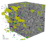
Discover how integrating micro-CT and plasma FIB-SEM enables multiscale 3D characterization of heterogeneous materials, linking structure, and performance.
Read more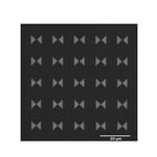
Learn how to reduce EBL stitching errors on a standard SEM using technological layers and smart write-field placement in a GDSII workflow.
Read more
Watch the recording and learn how UniTOM HR 2 enables Dynamic-to-Detail micro-CT imaging and Panthera AI denoising in time-resolved experiments.
Read more
Watch Tescan’s webinar on focused ion beam implantation for diamond engineering, NV center creation and quantum technology workflows.
Read more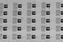
Learn practical methods to estimate lamella thickness for TEM, including FIB-SEM transparency, EELS-based measurement, and X-mark polishing techniques.
Read more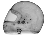
An interview with Riley Tejcek on performance and safety, including how non-destructive X-ray CT supports materials inspection in demanding environments.
Read more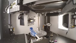
Join Tescan’s core facilities webinar to learn how PFIB-SEM, SEM, and micro-CT enable high-impact materials research in shared infrastructures.
Read more
Carlyle and other shareholders have entered into an agreement with Shimadzu Corporation that may result in a change in Tescan’s shareholding structure, subject to approvals.
Read more
Dr. Tatiana Gorelik shares insights on 3D electron diffraction, data acquisition strategies, and how new instrumentation shapes crystallography research.
Read more
Carlyle and Shimadzu Corporation have signed an agreement under which Tescan would become part of Shimadzu, subject to regulatory and customary approvals. The transaction has not yet closed.
Read more
Tescan announces a definitive agreement between Carlyle, its co-shareholders, and Shimadzu Corporation for the sale of the company, pending regulatory approval.
Read more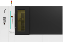
The University of Defence in Brno installs Tescan UNITOM XL microCT for ballistic protection, composite materials research, and advanced 3D material analysis.
Read more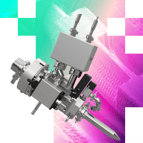
Discover how Tescan ORAGE 2 improves TEM lamella preparation with smarter automation, up to 40% faster processing, and reliable results for advanced semiconductor analysis.
Read more
Tescan and Wirsam co-hosted a hands-on Mineralogy Workshop in Johannesburg, uniting TIMA users to share insights on automated mineralogy and data optimization.
Read more
Czech Technical University enhances construction materials research with the Tescan AMBER X FIB-SEM, unlocking advanced microstructure analysis and 3D tomography capabilities.
Read more
Watch how plasma FIB-SEM on Tescan AMBER X 2 enables high-quality, artefact-free APT sample preparation and advanced nanoscale 3D characterization.
Read more
SGS celebrates the 100th TESCAN TIMA installation in Chile, advancing automated mineralogy and high-throughput mineral characterization.
Read more
Tescan and Dragonfly Energy showcase how advanced microscopy and data analytics accelerate lithium-ion battery innovation and sustainable manufacturing.
Read more
Turn your SEM into a nanofabrication powerhouse. Learn how researchers are patterning, depositing, and etching at the nanoscale–fast–using Tescan’s Nanoprototyping Toolbox and advanced SEM workflows.
Read more
Tescan supports the new Plasma FIB-SEM laboratory at CTU Prague, advancing materials science research and innovation in civil engineering.
Read more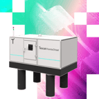
Tescan introduces the FemtoChisel femtosecond laser platform, delivering faster, more precise semiconductor sample preparation and integrated workflow performance.
Read more
Discover how Tescan FemtoChisel laser technology improves semiconductor sample preparation with greater speed, precision and workflow efficiency.
Read more
Discover how Tescan’s cryo-electron microscopy workflow helped uncover algae’s adaptive response to ZnO nanoparticles in collaboration with Mendel University.
Read more
Use Spectral CT to visualize internal battery and electronics structures. Detect delamination, misalignment, and material separation - fully non-destructively.
Read more
Tescan will join the Cryo-Microscopy Group Meeting at the University of Nottingham to showcase its Cryo SOLARIS X² system and latest cryo-microscopy innovations for life sciences.
Read moreGeometallurgy combines geological, mineralogical, and metallurgical data to predict how ore variability affects processing. This integrated approach improves resource modeling, reduces operational risk, and supports more efficient, sustainable, and profitable mining decisions.
Read more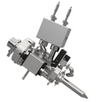
Learn how the new Tescan Orage™ 2 Ga⁺ FIB column combines higher milling speed, beam stability, and superior low keV image clarity to turn challenging TEM lamella preparation into a simple, reliable routine.
Read more
Highlights from the 3rd Tescan Collaboration Network Meeting at ER-C
Read more
Discover how Tescan EXLO™ improves TEM sample preparation with ex situ lift-out. Watch the on-demand webinar to increase throughput and reduce FIB time.
Read more
Explore real-world workflows using TESCAN AMBER X2 for semiconductor and battery research. Co-hosted with the University of Sydney.
Read more
Join us for the global launch of the MIRA XR SEM. Discover new levels of high-throughput, AI-driven imaging with real-world applications across materials and life sciences.
Read more
University of Leeds and RMS hosted a 4D-STEM & 3D-ED workshop, featuring TENSOR demos, keynotes from global experts, and interactive scientific sessions.
Read more
Tescan Group today announced the acquisition of FemtoInnovations and the creation of a dedicated Laser Technology Business Unit (LT BU).
Read more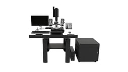
Discover how Tescan EXLO streamlines TEM specimen preparation with faster lift-out, improved workflow efficiency, and scalable processing for materials science and semiconductor labs.
Read moreInterview with Jean-Charles Chen, CEO of Tescan Group: Unveiling a New Era of Discovery
Read moreDiscover how Tescan CEO Jean-Charles Chen explains the company’s rebranding, strategic priorities, and vision for the future of scientific discovery.
Read more
TESCAN’s AMBER X 2 Plasma FIB-SEM wins the 2025 R&D 100 Award for combining high-throughput 3D analysis with nanometer-precision TEM specimen prep.
Read more
TESCAN will co-host a collaborative webinar with the University of Leeds, presenting a low-dose 4D-STEM methodology for characterising beam-sensitive polymers and soft matter.
Read moreNo items match the selected filters.