Accelerating the Art
of Discovery
FemtoChisel for high-precision semiconductor sample prep

Tescan Solutions

Explore Materials Science at Micro and Nano Scale with Precision
Analyze structure, defects and interfaces using FIB-SEM, STEM and micro-CT systems built to support every stage from R&D to production. Use these tools to ensure consistency throughout your workflow.
Advance Semiconductor Failure Analysis with Confidence
Ensure device integrity and consistent results throughout various analysis phases. Our solutions support precise delayering, TEM lamella preparation, non-destructive 3D imaging, and package-level cross-sectioning. They help isolate faults, validate advanced packaging, and identify root causes reliably. Automated workflows and precise endpointing provide clarity and uniformity, helping you make quicker decisions and improve device performance.
%20(1).webp?width=500&height=250&name=Frame%20722%20(1)%20(1).webp)
Advance Battery Research and Production with Confidence
Deliver reliable insights throughout the energy storage lifecycle, from raw material optimization to cell design and recycling. Our comprehensive workflows integrate high-resolution imaging, multimodal analysis, and non-destructive 3D visualization to uncover particle morphology, electrode interfaces, and failure mechanisms, all while maintaining sample integrity. Automated workflows deliver reproducible data that improve quality assurance, accelerate innovation, and promote sustainability in advanced battery technologies.
.webp?width=500&height=250&name=Frame%20722%20(3).webp)
Explore Life Sciences at Native State with Confidence
Preserve cellular and tissue structures with cryogenic FIB-SEM workflows for precise biological analysis. Covering cryo-ET sample prep, surface morphology, and 3D volume reconstruction, our tools assist multiple phases of life science research. Consistent cryogenic conditions, automated milling, and accurate imaging preserve structural integrity, providing reproducible, high-resolution data for better biological system insights.
%20(1).webp?width=500&height=250&name=Frame%20722%20(2)%20(1).webp)
Explore Geoscience in 2D and 3D with Clarity
Advance geoscience research with integrated imaging and analysis solutions built for the complexity of natural materials. Tescan Micro-CT systems reveal 3D pore networks, textures, and fossils structures with exceptional resolution, while SEM-based mineralogical analysis quantifies mineralphases, grain relationships, and chemical composition. From petrology and paleontology to reservoir evaluation, CO2 and H2 storage, and mineral processing, these complementary techniques deliver reproducible, quantitative insights that link microstructure to behavior – empowering confident, data-driven interpretations across the geosciences.

Explore Materials Science at Micro and Nano Scale with Precision
Analyze structure, defects and interfaces using FIB-SEM, STEM and micro-CT systems built to support every stage from R&D to production. Use these tools to ensure consistency throughout your workflow.
Advance Semiconductor Failure Analysis with Confidence
Ensure device integrity and consistent results throughout various analysis phases. Our solutions support precise delayering, TEM lamella preparation, non-destructive 3D imaging, and package-level cross-sectioning. They help isolate faults, validate advanced packaging, and identify root causes reliably. Automated workflows and precise endpointing provide clarity and uniformity, helping you make quicker decisions and improve device performance.
%20(1).webp?width=500&height=250&name=Frame%20722%20(1)%20(1).webp)
Advance Battery Research and Production with Confidence
Deliver reliable insights throughout the energy storage lifecycle, from raw material optimization to cell design and recycling. Our comprehensive workflows integrate high-resolution imaging, multimodal analysis, and non-destructive 3D visualization to uncover particle morphology, electrode interfaces, and failure mechanisms, all while maintaining sample integrity. Automated workflows deliver reproducible data that improve quality assurance, accelerate innovation, and promote sustainability in advanced battery technologies.
.webp?width=500&height=250&name=Frame%20722%20(3).webp)
Explore Life Sciences at Native State with Confidence
Preserve cellular and tissue structures with cryogenic FIB-SEM workflows for precise biological analysis. Covering cryo-ET sample prep, surface morphology, and 3D volume reconstruction, our tools assist multiple phases of life science research. Consistent cryogenic conditions, automated milling, and accurate imaging preserve structural integrity, providing reproducible, high-resolution data for better biological system insights.
%20(1).webp?width=500&height=250&name=Frame%20722%20(2)%20(1).webp)
Explore Geoscience in 2D and 3D with Clarity
Advance geoscience research with integrated imaging and analysis solutions built for the complexity of natural materials. Tescan Micro-CT systems reveal 3D pore networks, textures, and fossils structures with exceptional resolution, while SEM-based mineralogical analysis quantifies mineralphases, grain relationships, and chemical composition. From petrology and paleontology to reservoir evaluation, CO2 and H2 storage, and mineral processing, these complementary techniques deliver reproducible, quantitative insights that link microstructure to behavior – empowering confident, data-driven interpretations across the geosciences.
Accelerating science
What Is STEM? TEM vs STEM, 4D-STEM & Electron Diffraction Explained
Learn what STEM (Scanning Transmission Electron Microscopy) is, how it works, and how it compares to TEM. Explore 4D-STEM, electron diffraction, and analytical techniques for materials and semiconductors.
INDICO FEBID & FIBID Workshop | Advancing 3D Nanoprinting
The INDICO FEBID workshop in Frankfurt advanced digital control for reliable 3D nanoprinting. Tescan contributed expertise in SEM-based nanofabrication, FIBID and in situ process monitoring.
Interview | Micro-CT Imaging in Prenatal Care | Early Human Development
Discover how micro-CT imaging is transforming prenatal care and early human development research through non-destructive, high-resolution 3D anatomical analysis.
Interview | Andy Brown - 4D-STEM for Beam-Sensitive Materials
Discover how 4D-STEM and TESCAN TENSOR enable dose-efficient analysis of beam-sensitive materials, advancing electron diffraction and structural research.
Enroll
.webp?width=1201&height=802&name=MIRA%20XR%20GM%20MONO%20Metal%20(3).webp)
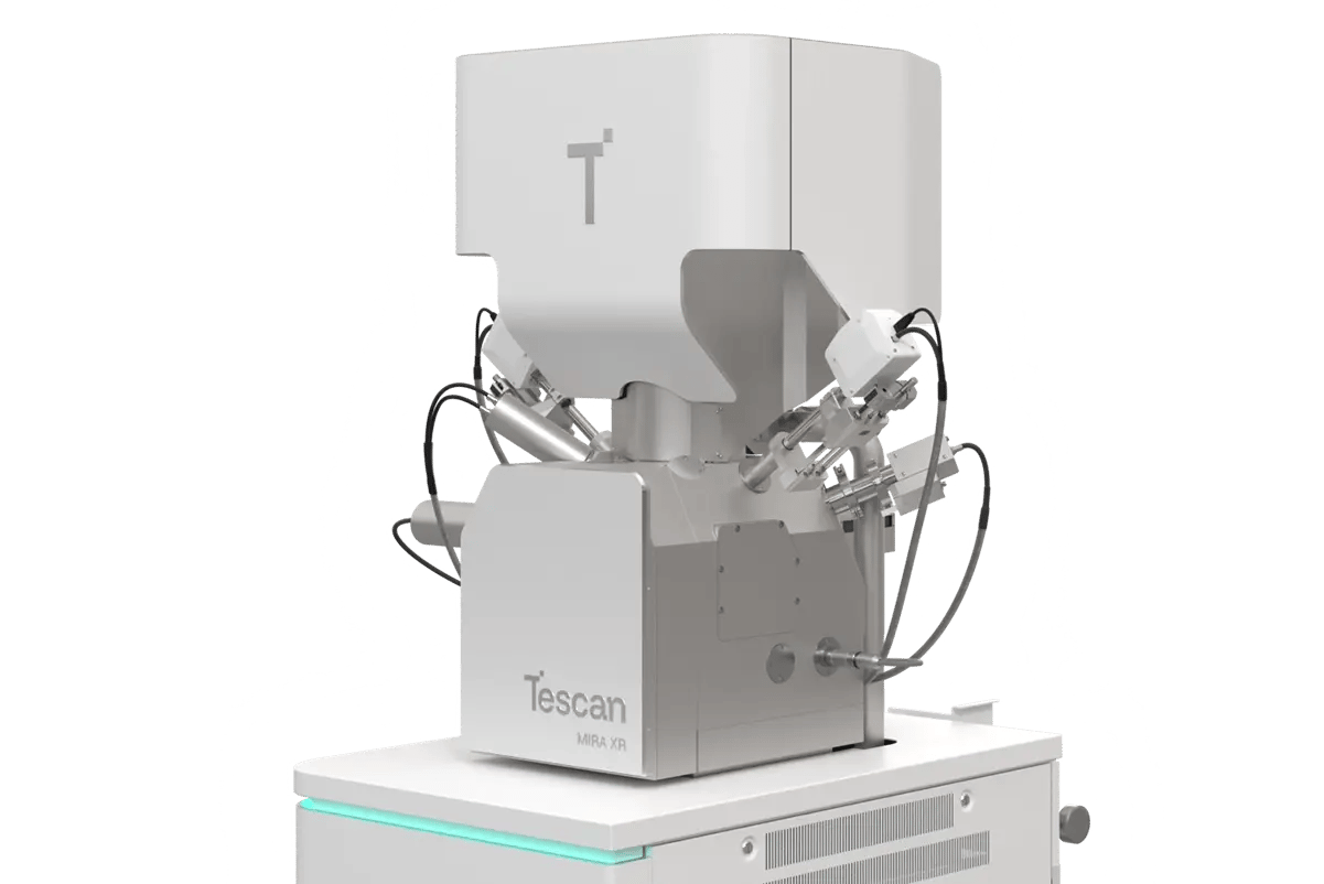
SEM Platforms for Clear, Reproducible Insight
Tescan’s SEM platforms provide high-resolution imaging and surface analysis with exceptional contrast, detail, and ease of use—ideal for materials research, quality control, and analytical applications.

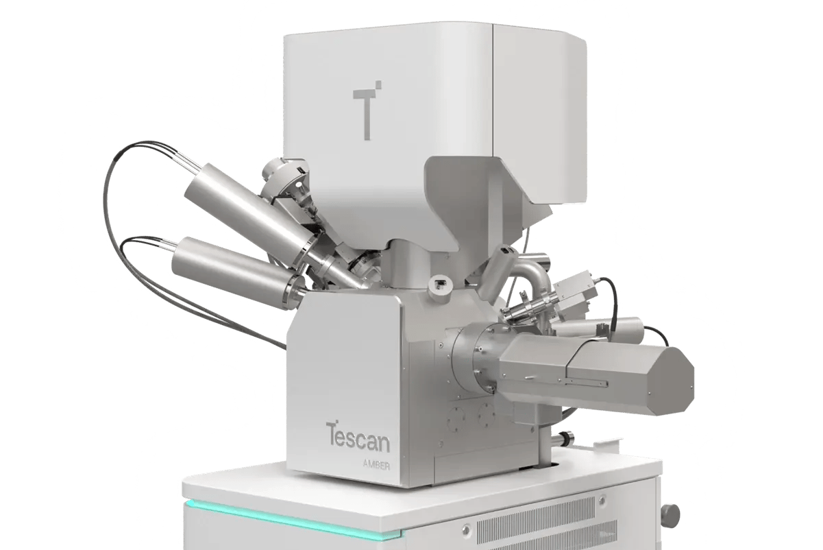
Advanced FIB-SEM for Insight and Impact
Tescan FIB-SEM systems combine fast, precise milling with high-resolution imaging and advanced automation. Choose from Ga or Xe plasma FIB sources to match your needs in sample prep, prototyping, or failure analysis.

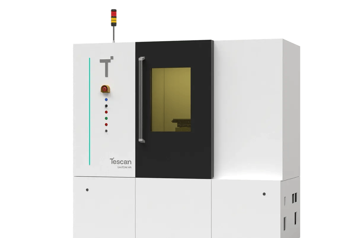
Dynamic MicroCT for Structural and Material Insight
Tescan’s X-ray micro-CT systems deliver fast, high-resolution 3D and 4D imaging for non-destructive internal analysis. Dynamic in-situ capabilities and modular designs make them ideal for advanced research across materials, life sciences, and energy storage.

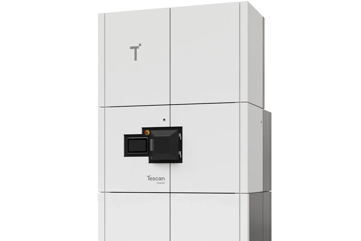
Nanoscale Insights with Tescan TENSOR Analytical STEM
Tescan's TENSOR is the first 4D-STEM platform built for intuitive multimodal nanocharacterization, combining structural, morphological, and chemical insights in every scan. Real-time data processing, automation, and scripting support make it ideal for both routine and advanced research
%20(1)%20(1)%20(1).webp?width=1201&height=802&name=FemtoChisel-Exterior-Chrome-no-background%20(6)%20(1)%20(1)%20(1).webp)
FemtoChisel for High-Precision Semiconductor Sample Prep
FemtoChisel is the next-generation femtosecond laser solution built specifically for semiconductor sample preparation and failure analysis. For too long, the industry has had to compromise between throughput, precision, and Surface Quality. Now all are delivered on one integrated platform.
.webp?width=1201&height=802&name=Nov%C3%BD%20projekt%20(23).webp)
Fast, Precise Ex Situ Lift-Out with Tescan EXLO
Tescan EXLO is designed for laboratories where TEM throughput, reproducibility, and cost efficiency matter. By moving specimen lift-out outside the FIB-SEM, EXLO keeps valuable beam time focused on milling, while parallelizing lamella transfer and grid mounting. The result: higher output, lower cost per specimen, and a more efficient workflow.
.webp?width=1201&height=802&name=Nov%C3%BD%20projekt%20(24).webp)
High-Precision Systems for Ion Implantation and UHV Research
Tescan’s advanced systems support operation under demanding conditions-from controlled ion implantation to analytical tasks performed in ultra-high vacuum environments-while offering the freedom to customize system configuration and workflows to your specific research needs.
Discover the power of Tescan instruments
.webp?width=1201&height=802&name=MIRA%20XR%20GM%20MONO%20Metal%20(3).webp)
SEM Platforms for Clear, Reproducible Insight
Tescan’s SEM platforms provide high-resolution imaging and surface analysis with exceptional contrast, detail, and ease of use—ideal for materials research, quality control, and analytical applications.

Advanced FIB-SEM for Insight and Impact
Tescan FIB-SEM systems combine fast, precise milling with high-resolution imaging and advanced automation. Choose from Ga or Xe plasma FIB sources to match your needs in sample prep, prototyping, or failure analysis.

Dynamic MicroCT for Structural and Material Insight
Tescan’s X-ray micro-CT systems deliver fast, high-resolution 3D and 4D imaging for non-destructive internal analysis. Dynamic in-situ capabilities and modular designs make them ideal for advanced research across materials, life sciences, and energy storage.

Nanoscale Insights with Tescan TENSOR Analytical STEM
Tescan's TENSOR is the first 4D-STEM platform built for intuitive multimodal nanocharacterization, combining structural, morphological, and chemical insights in every scan. Real-time data processing, automation, and scripting support make it ideal for both routine and advanced research
%20(1)%20(1)%20(1).webp?width=1201&height=802&name=FemtoChisel-Exterior-Chrome-no-background%20(6)%20(1)%20(1)%20(1).webp)
FemtoChisel for High-Precision Semiconductor Sample Prep
FemtoChisel is the next-generation femtosecond laser solution built specifically for semiconductor sample preparation and failure analysis. For too long, the industry has had to compromise between throughput, precision, and Surface Quality. Now all are delivered on one integrated platform.
.webp?width=1201&height=802&name=Nov%C3%BD%20projekt%20(23).webp)
Fast, Precise Ex Situ Lift-Out with Tescan EXLO
Tescan EXLO is designed for laboratories where TEM throughput, reproducibility, and cost efficiency matter. By moving specimen lift-out outside the FIB-SEM, EXLO keeps valuable beam time focused on milling, while parallelizing lamella transfer and grid mounting. The result: higher output, lower cost per specimen, and a more efficient workflow.
.webp?width=1201&height=802&name=Nov%C3%BD%20projekt%20(24).webp)
High-Precision Systems for Ion Implantation and UHV Research
Tescan’s advanced systems support operation under demanding conditions-from controlled ion implantation to analytical tasks performed in ultra-high vacuum environments-while offering the freedom to customize system configuration and workflows to your specific research needs.
Discover the power

Scanning Electron Microscopes (SEM)
Tescan’s SEM platforms provide high-resolution imaging and surface analysis with exceptional contrast, detail, and ease of use—ideal for materials research, quality control, and analytical applications.

Focused Ion Beam-Scanning Electron Microscopes (FIB-SEM)
Tescan FIB-SEM systems combine fast, precise milling with high-resolution imaging and advanced automation. Choose from Ga or Xe plasma FIB sources to match your needs in sample prep, prototyping, or failure analysis.

Micro-computed tomography (microCT)
Tescan’s X-ray micro-CT systems deliver fast, high-resolution 3D and 4D imaging for non-destructive internal analysis. Dynamic in-situ capabilities and modular designs make them ideal for advanced research across materials, life sciences, and energy storage.

4D STEM
Tescan's TENSOR is the first 4D-STEM platform built for intuitive multimodal nanocharacterization, combining structural, morphological, and chemical insights in every scan. Real-time data processing, automation, and scripting support make it ideal for both routine and advanced research.

Laser solutions
FemtoChisel is the next-generation femtosecond laser solution built specifically for semiconductor sample preparation and failure analysis. For too long, the industry has had to compromise between throughput, precision, and Surface Quality. Now all are delivered on one integrated platform.

Ex Situ Lift-Out Solutions
Tescan EXLO is designed for laboratories where TEM throughput, reproducibility, and cost efficiency matter. By moving specimen lift-out outside the FIB-SEM, EXLO keeps valuable beam time focused on milling, while parallelizing lamella transfer and grid mounting. The result: higher output, lower cost per specimen, and a more efficient workflow.
.webp?width=415&height=400&name=NANOSPACE%20w600%20(1).webp)
Ion Implantation and UHV FIB-SEM Solutions
Tescan’s advanced systems support operation under demanding conditions-from controlled ion implantation to analytical tasks performed in ultra-high vacuum environments-while offering the freedom to customize system configuration and workflows to your specific research needs.
About Tescan
Decades of Progress, Just Getting Started
Since 1991, Tescan systems have been designed to feel seamless, intuitive, and built for real research. Think of us as reducing the coefficient of friction between question and discovery.

.png?width=500&height=700&name=_%20Content%20Image%20Size%206%20(1).png)
GET IN Touch

Where can you find us:
Tescan
Libušina třída 21
623 00 Brno
Czech Republic
No distributors found.

.png?width=500&height=600&name=Image%20Element%20(7).png)