Throughput at Every Scale
Achieve fast, large-area cross-sectioning with Xe Plasma FIB currents up to 3.3 µA—ideal for analyzing complex IC packages and stacked devices.
Deep Cross-Sectioning and Precision End-Pointing for Advanced Package Failure Analysis

Tescan SOLARIS X™ 2 is built for laboratories where package-level failure analysis, large-area cross-sectioning, and Ga-free sample preparation demand both speed and precision. Powered by the Mistral™ Xe Plasma FIB column, SOLARIS X™ 2 delivers high-current milling with exceptional surface quality, while the Triglav™ SEM column ensures nanometer-scale imaging accuracy at the beam coincidence point. The result: fast, artifact-free cross-sections and reliable results across advanced IC packages, MEMS, and display devices.

For materials science laboratories, Tescan SOLARIS X ™ 2 brings together two key advantages: the precise, high-throughput Mistral ™ plasma FIB column and Triglav ™ ultra-high-resolution SEM imaging. The combination is ideal for fabrication and characterization workflows that require fast processing of larger volumes without sacrificing visibility of very small features. It also enables rapid, site-specific TEM sample preparation and supports applications where avoiding Ga+ contamination is important.

Tescan SOLARIS X™ 2 equipped with the Nanoprototyping Toolbox delivers complete FIB-SEM capabilities for nanoscale device prototyping — from design to inspection — combining immersion-optics UHR-SEM imaging with gallium-free plasma FIB fabrication to create, modify, and analyse functional structures with unmatched clarity and material integrity.
Design and fabricate novel 2D/3D structures using both electron and ion beam — from plasmonic sensors to freestanding nanowires
Preserve material integrity and scale your prototyping freely from nanoscale features to micro-scale geometries — gallium-free Xe plasma FIB eliminates contamination without compromising precision at any feature size
Inspect and characterise your prototyped structures at ultra-high resolution with immersion-optics SEM — confirming that what you see reflects the true device, not fabrication artifacts
Accelerate prototyping cycles from weeks to hours — cross-section your fabricated devices in-situ, analyse dose, geometry, and material properties, and iterate without changing tools
Automate even complex prototyping routines end-to-end with Python API and block-based automation — no programming expertise required
Tescan SOLARIS X™ 2 extends nanoscale research capabilities with a fully integrated FIB-SEM environment for fabrication and analysis — one microscope, one software, total control. Its immersion-optics UHR-SEM delivers the imaging clarity needed to resolve the finest structural details, while gallium-free Xe plasma FIB ensures your prototyped devices retain their true material properties from nano to micro scale. Whether you're building photonic crystals, fabricating waveguide prototypes, or exploring gallium-sensitive quantum materials, SOLARIS X™ 2 supports fast, flexible, and contamination-free nanoscale innovation — with the imaging quality to verify every step.


Tescan Solaris X™ 2 extends FIB physical failure analysis to advanced device architectures including 2.5D and 3D ICs, flip-chips, and HBM modules. Engineers can expose sub-surface features such as cracks, voids, and delaminations with exceptional precision, ensuring faster root-cause identification and reproducible process control in semiconductor manufacturing and packaging R&D.

For MEMS research and failure analysis, SOLARIS X™ 2 combines high-current Xe Plasma FIB with artifact-suppression technology to reveal buried interfaces and micro-scale geometries in detail.
The system supports development and quality assessment of sensors, actuators, and other 3D microsystems where milling precision and clean sectioning are critical.

For display manufacturers and materials researchers, Solaris X™ 2 enables detailed inspection of pixel arrays, contact interfaces, and encapsulation layers. Deep sectioning with inert Xe ions preserves delicate thin-film structures, ensuring accurate visualization of electrical, optical, and mechanical defects within next-generation display technologies.

Tescan Solaris X™ 2 supports precise structural and compositional analysis of complex optoelectronic assemblies. Its combination of sharp Xe Plasma FIB milling and sensitive SEM imaging enables engineers to investigate layer bonding, defect propagation, and structural alignment within photonic and light-emitting devices.

With its high resolution Xe Plasma FIB and precise beam control, Solaris X™ 2 streamlines TEM specimen preparation for semiconductor and materials applications. The Ga-free workflow eliminates contamination and preserves true microstructural integrity, ensuring accurate characterization in STEM, EDS, and EBSD studies.


Explore biological structures across large volumes without sacrificing nanoscale detail. Tescan SOLARIS X™ 2 combines ultra‑high‑resolution SEM immersion optics with a powerful Xe plasma FIB to deliver clean cross‑sections and advanced room‑temperature and cryogenic workflows for life‑science research.
Tescan SOLARIS X™ 2 is the solution of choice for life scientists who require imaging excellence first, backed by powerful, precise plasma FIB milling—from routine room‑temperature analysis to the most demanding cryogenic applications.

High-precision Plasma FIB-SEM for physical failure analysis and process validation
Deep cross-sectioning up to 1 mm for package-level defect localization
Nanometer-precision end-pointing at the FIB–SEM coincidence point
Ga-free TEM lamella preparation for reliable downstream analysis
Tescan Solaris X 2 extends FIB physical failure analysis to advanced device architectures including 2.5D and 3D ICs, flip-chips, and HBM modules. Engineers can expose sub-surface features such as cracks, voids, and delaminations with exceptional precision, ensuring faster root-cause identification and reproducible process control in semiconductor manufacturing and packaging R&D.
Accurate cross-sectioning and high-resolution imaging for complex 3D microstructures
Xe Plasma FIB milling for fast, large-volume cross-sections
Artifact-free polishing using TRUE X-sectioning and Rocking Stage technologies
Damage-free analysis of micro-scale mechanical structures
For MEMS research and failure analysis, SOLARIS X 2 combines high-current Xe Plasma FIB with artifact-suppression technology to reveal buried interfaces and microactuator geometries in detail. The system supports development and quality assessment of sensors, actuators, and other 3D microsystems where mechanical precision and clean sectioning are critical.
Large-area FIB-SEM for analyzing thin-film and multilayer display stacks
High-throughput cross-sectioning of OLED and TFT displays
Precise end-pointing across complex layered structures
Reliable imaging of conductive and beam-sensitive materials
For display manufacturers and materials researchers, SOLARIS X 2 enables detailed inspection of pixel arrays, contact interfaces, and encapsulation layers. Deep sectioning with inert Xe ions preserves delicate thin-film structures, ensuring accurate visualization of electrical, optical, and mechanical defects within next-generation display technologies.
High-resolution imaging and cross-sectioning for optical and photonic components
Clean sectioning of LEDs, VCSELs, and laser diodes
High-contrast SEM imaging for optical interface evaluation
Ga-free milling preserves active optical layers and coatings
Tescan Solaris X 2 supports precise structural and compositional analysis of complex optoelectronic assemblies. Its combination of sharp Xe Plasma FIB milling and sensitive SEM imaging enables engineers to investigate layer bonding, defect propagation, and structural alignment within photonic and light-emitting devices.
Efficient, Ga-free sample preparation for high-quality TEM and STEM analysis
Automated lamella thinning under 100 nm
Inert Xe ions prevent implantation and sample contamination
Optimized for sub-surface target exposure in complex devices
With its high resolutionXe Plasma FIB and precise beam control, SOLARIS X 2 streamlines TEM specimen preparation for semiconductor and materials applications. The Ga-free workflow eliminates contamination and preserves true microstructural integrity, ensuring accurate characterization in STEM, EDS, and EBSD studies.
Large-volume 3D microanalysis for advanced materials and composites
Combined 3D EDS and EBSD for composition and crystallography
Artifact-free sectioning of ceramics, polymers, and glass materials
Fast, automated reconstruction for structural and chemical mapping
Beyond semiconductor analysis, SOLARIS X 2 provides powerful 3D analytical capabilities for diverse materials research. Its plasma FIB-SEM workflow enables correlative microanalysis at multiple scales—capturing the chemical, structural, and crystallographic details that drive innovation in materials science and engineering.

Tescan SOLARIS X 2 combines Mistral™ Xe plasma FIB with UHR-SEM immersion optics for precise lamella preparation and high-quality volume imaging. Its enhanced beam profile enables fast milling and low-energy polishing, ideal for large-volume and high-throughput cryo workflows.
Mistral™ Xe Plasma FIB Column: Enhanced beam profile for fast milling and precise low-energy polishing.
UHR-SEM Immersion Optics: Optimized for high-quality cryo imaging.
Integrated Leica/Quorum cryo workflow
Built-in Tescan Cryo-Nanomanipulator: Temperature-controlled system for safe and efficient lamella lift-out
Integrated CLEM: Precise ROI targeting with integrated METEOR 2.0
Tescan Essence™ Software: Designed for multi-user environments, ensuring effortless operation regardless of experience level.
From comprehensive cryo electron tomography sample preparation to high-quality cryo volume imaging enabled by immersion-SEM optics, SOLARIS X2 integrates every tool needed for advanced structural biology research.
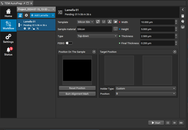
TEM AutoPrep™ Pro is integrated into the Tescan SOLARIS X™ 2 platform, automating TEM lamella preparation from trenching to final thinning with minimal manual input. Paired with Tescan EXLO™, preparation and extraction run in parallel to maximize beam utilization, reduce turnaround time, and deliver consistent, high-quality results.
Operators benefit from guided automation, motorized precision, and real-time imaging within the Essence™ user interface. Automated alignment and intuitive controls reduce setup time and user variability, making SOLARIS X™ 2 and Tescan TEM AutoPrep™ Pro a scalable, high-throughput solution for reproducible TEM sample preparation.