.png?width=1131&height=979&name=N%C3%A1vrh%20bez%20n%C3%A1zvu%20(1).png)
Achieve Pristine Laser Surfaces for Faster Semiconductor Analysis
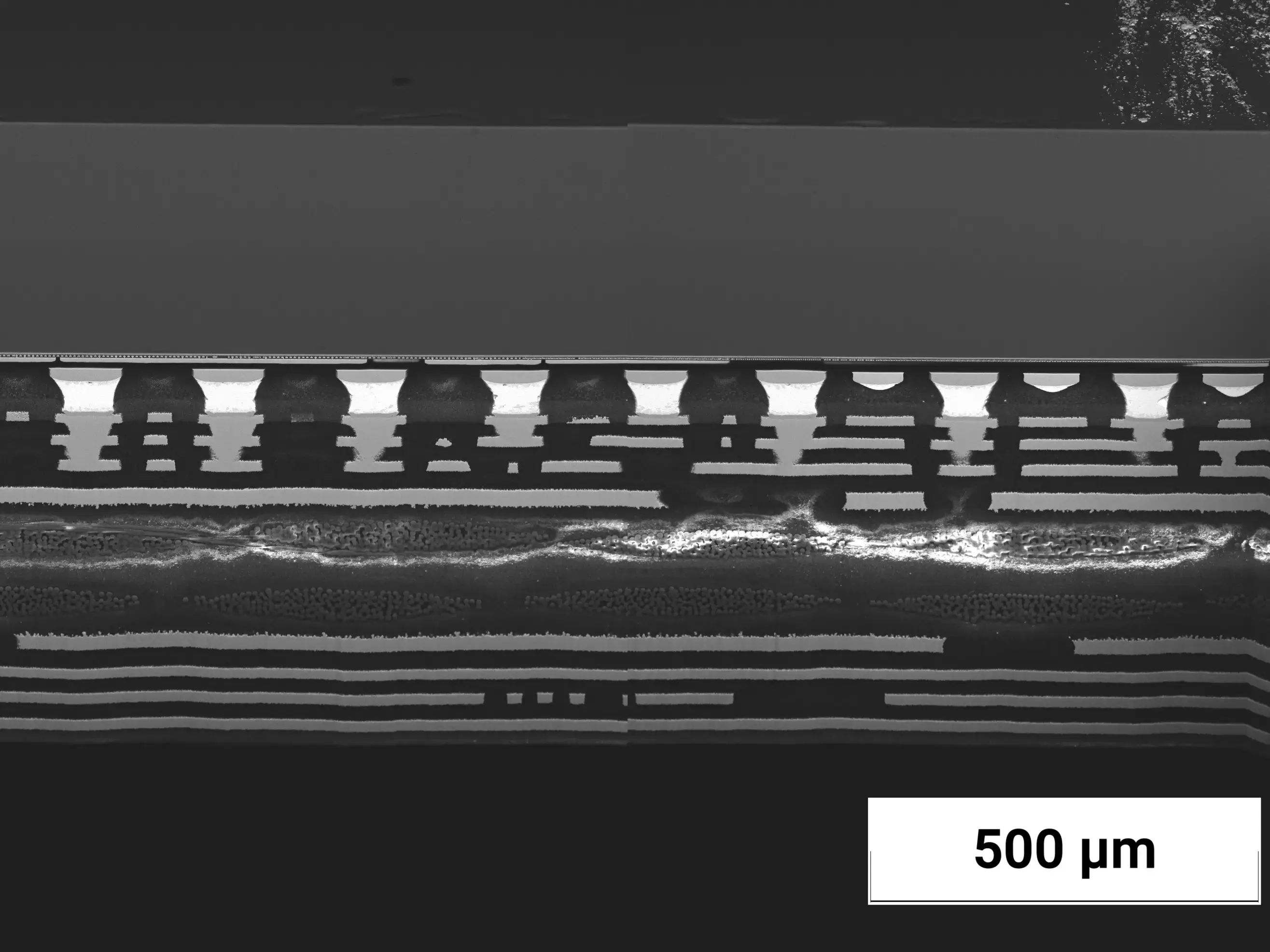
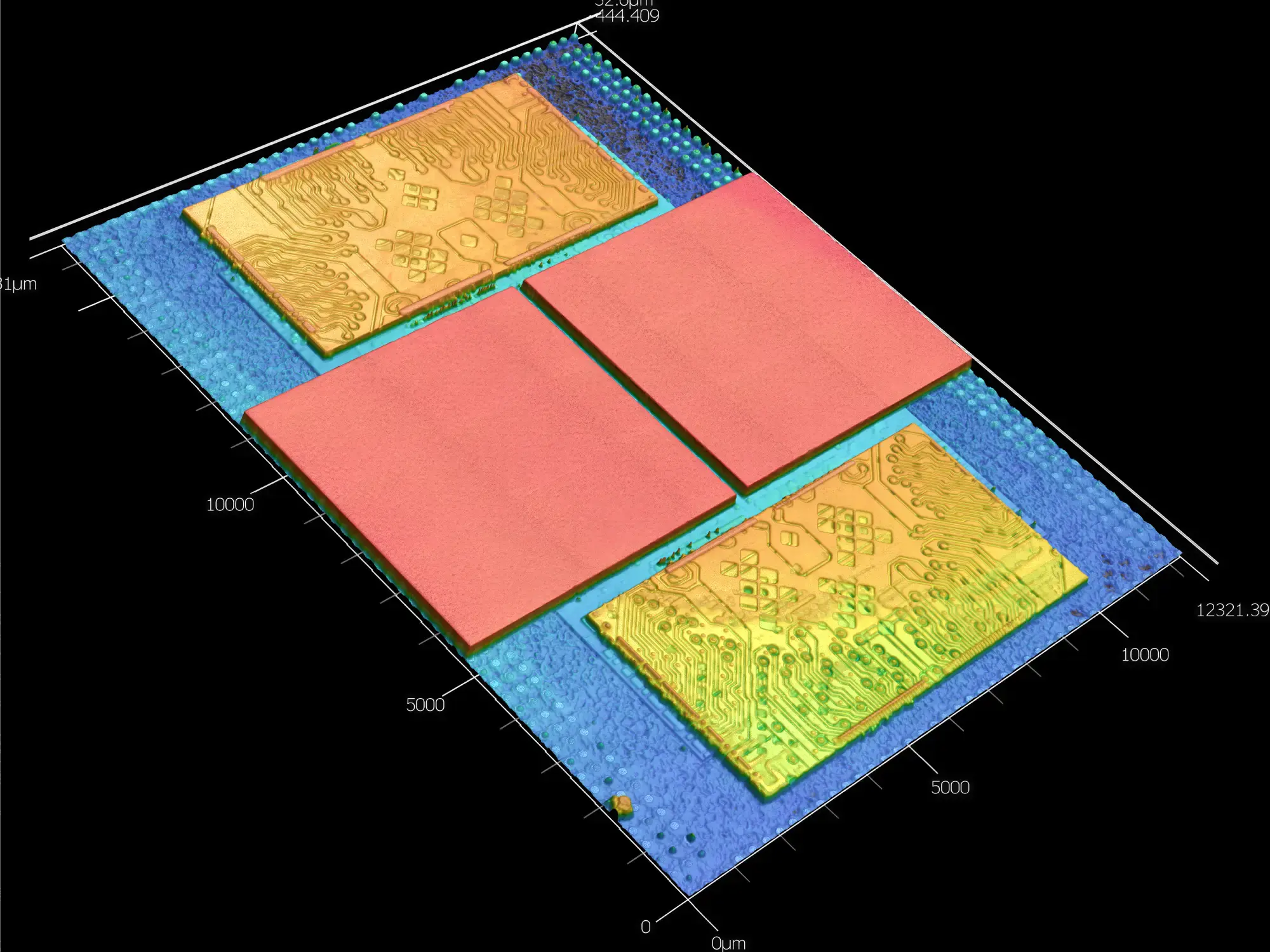
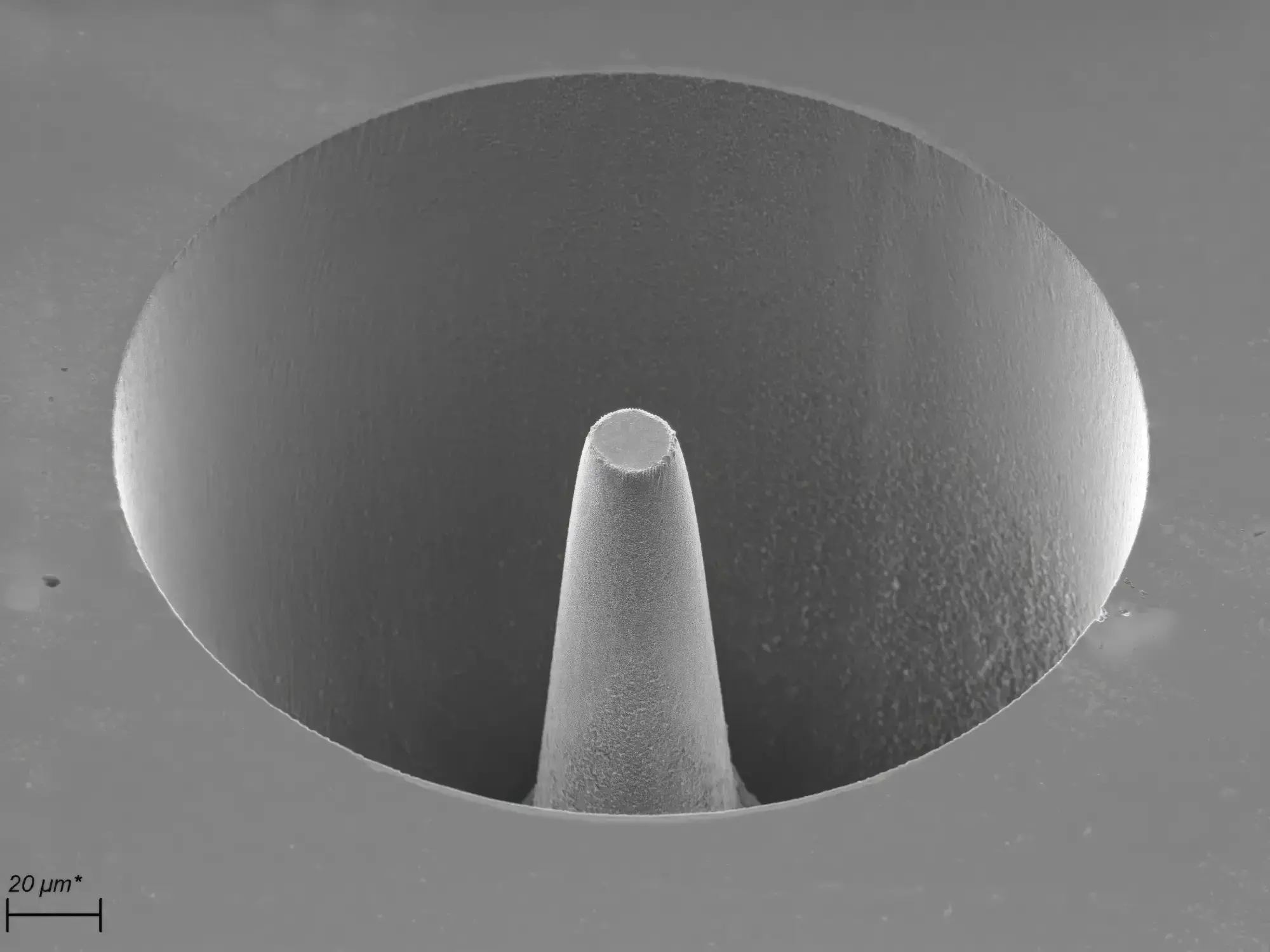
Tescan FemtoChisel™ is a femtosecond laser micro and nano machining system for sample preparation, micro and nano fabrication, failure analysis, and surface modification. Designed for semiconductor, glass processing, materials research, and biomedical device manufacturing workflows, it helps users access buried regions of interest, prepare clean surfaces, and accelerate analysis.
Key benefits
- Intelligent Multi-Gas Processing
- Laser Protective Layer
- Multi degrees of freedom stage with tilt and wafer-level rotation
- Correlative Machine Vision & Targeting
- Software-Selectable Laser Wavelength
- Real-time surface and ablation monitoring with material adaptability