WEBINAR | Up to 40% Faster Automated TEM Lamella Preparation with new Ga⁺ FIB Column

Tescan MIRA XR

MIRA XR
MIRA XR

Tescan MIRA XR supports SEM workflows that rely on clarity, consistency and confident decision-making. Its BrightBeam™ optics, Axial detector, Wide Field Optics™ and Essence™ SW give materials scientists and inspection teams the accuracy they need from first image to final check.

Achieve smoother daily imaging with stable performance, clear navigation and efficient shifts between imaging and microanalysis.

  • Navigate complex or tilted samples with Wide Field Optics™ offering a clear overview at low magnification

  • Maintain stable conditions with In-Flight™ automated beam control

  • Capture surface detail at low landing energies using the BrightBeam™ field-free column

  • Acquire EDS spectra and maps directly in the SEM window through Essence™ EDS

  • Work confidently with uncoated samples using MultiVac variable pressure imaging

  • Adapt workflows with Axial SE/BSE detection and optional retractable BSE detectors

How TESCAN MIRA XR

Enhances SEM Solutions

Clear Low-keV Imaging with BrightBeam™ Optics

Achieve stable, field-free performance at low voltages with BrightBeam™ electrostatic–magnetic lenses. This supports detailed surface imaging on sensitive or magnetic materials without constant adjustment.

Consistent Beam Conditions with In-Flight™ Automated Controls

Maintain reliable beam conditions as In-Flight™ Beam Tracing and other automatic functions adjust key parameters automatically during transitions. It shortens setup time and supports consistent results across users.

Integrated SEM–EDS for Efficient Microanalysis

Collect spectra, maps and profiles inside the SEM workspace through Essence™ EDS. Structural and compositional insight stays connected without switching applications.

Reliable Navigation with Wide Field Optics™

Locate regions of interest quickly using an undistorted SEM overview from 2× magnification. Wide Field Optics™ helps you orient and revisit features on large or tilted samples.

Variable Pressure Imaging for Challenging Samples

Image non-conductive or outgassing materials using MultiVac variable pressure. The gaseous SE detector enhances topography at low keV without modifying sensitive surfaces.

Versatile Detection for Materials and Topography

Capture SE and BSE signals efficiently with the Axial detector for surface and material contrast. Optional retractable BSE detectors extend capability across different voltages and materials.

Tescan Essence™

Unified Control for SEM Imaging and Microanalysis

Essence™ brings imaging, navigation and analytical tools into one environment, supporting clear, consistent SEM workflows for materials scientists and inspection teams. Its streamlined layout and automation features help users move efficiently from first navigation to final verification.

  • Access live spectra, maps and profiles through integrated Essence™ EDS
  • Maintain stable imaging conditions with In-Flight™ automated routines
  • Protect detectors and samples using the real-time 3D Collision Model

Tescan MIRA XR Applications

_ Application area icon
Tescan MIRA XR in Materials Science

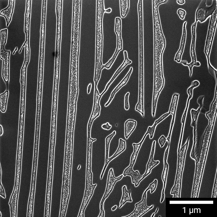
High-resolution SEM imaging across diverse material classes

  • Examine surface morphology using stable SE imaging at low landing energies
  • Differentiate phases and structures with Axial and retractable BSE detection
  • Correlate composition with integrated Essence™ EDS
  • Navigate large or multi-angle specimens with Wide Field Optics™

Researchers rely on MIRA XR for precise imaging of microstructures, interfaces and defects in metals, ceramics, polymers and composites. The system maintains consistent beam performance and integrates SEM–EDS in one workspace, helping you move efficiently from first inspection to clear insight.

Tescan MIRA XR in in Industrial Inspection & Quality Control

Fast, confident surface and compositional assessment

  • Identify surface features and defects with high-contrast SE and BSE imaging
  • Assess coatings, fractures and interfaces with stable low-keV performance
  • Carry out quick composition checks using Essence™ EDS
  • Work with larger parts using the spacious chamber and flexible stage travel

Inspection teams use MIRA XR to verify components, monitor manufacturing variation and identify failure modes. Reliable variable pressure imaging and short transitions between imaging and EDS support faster, more consistent evaluations.

Application area=SC
Tescan MIRA XR in Semiconductors

SEM accessibility for shared environments

  • Begin with a clear overview using Wide Field Optics™
  • Support different experience levels with customizable Essence™ layouts
  • Protect detectors and samples using the Essence™ 3D Collision Model
  • Expand capability with optional BSE or correlative modules

Universities and research centres choose MIRA XR for its balanced combination of usability, stability and analytical flexibility. It helps teams progress varied projects without compromising data quality or workflow efficiency.

Unlocked content

Unlock
Tescan insight

leave a contact to access

Get the most out of Tescan

This is more than information; it's an advantage. We've compiled our technical whitepapers, detailed product flyers, and on-demand webinars to provide you with the knowledge that makes a real difference. Sign up now to access the insights you need to make an impact.

Tescan MIRA XR

Technical specification

Tescan MIRA XR

MIRA XR Platform
  • BrightBeam™ field-free UHR SEM column for stable low-keV imaging
  • High-resolution surface analysis down to ~1.4 nm at 30 kV
  • Wide Field Optics™ for low-magnification SEM overview starting at 2×
  • Integrated SEM imaging and navigation within Tescan Essence™
Imaging and Analysis
  • In-Column Axial SE/BSE detector for efficient topographic and material contrast
  • Chamber SE detection for conventional high-vacuum imaging
  • Optional retractable BSE detectors (LE-RBSE, 4Q-BSE) for analytical contrast
  • Integrated Essence™ EDS for spectra, mapping and line profiles in the SEM window
Vacuum and Sample Handling
  • High-vacuum imaging for fine topographic detail
  • MultiVac variable pressure mode for non-conductive and outgassing samples
  • Gaseous SE detector (GSD) for enhanced low-keV topography in VP mode
  • Flexible sample chamber supporting large and tilted specimens
Stage and Navigation
  • Motorized 5-axis Compucentric stage with precise positioning
  • Wide Field Optics™ for confident sample navigation and ROI recovery
  • Essence™ 3D Collision Model for safe stage movement and detector protection
Automation and User Support
  • In-Flight™ automated beam optimization for stable, repeatable imaging
  • Recipe-driven SEM routines for consistent workflows across users
  • Essence™ interface with customizable layouts for multi-user facilities
Software and Workflow Integration
  • Tescan Essence™ for unified imaging, EDS, navigation and system control
  • Dual Essence™ EDS for integrated microanalysis
  • Support for optional modules including Image Snapper and SharkSEM Advanced (where configured)
MIRA XR 2

GET IN Touch

Contact us

map

Where you can find us:

Tescan Brno
Libušina třída 21
623 00 Brno
Czech Republic


info@Tescan.com