
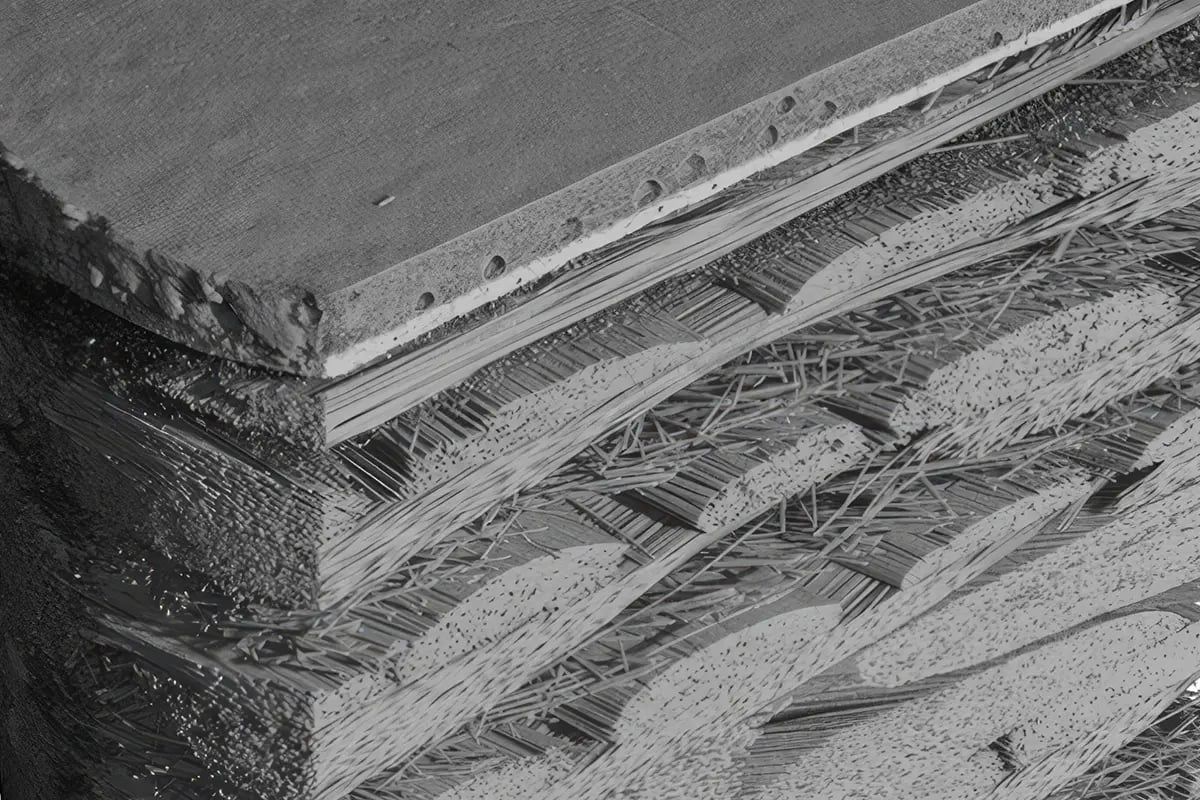
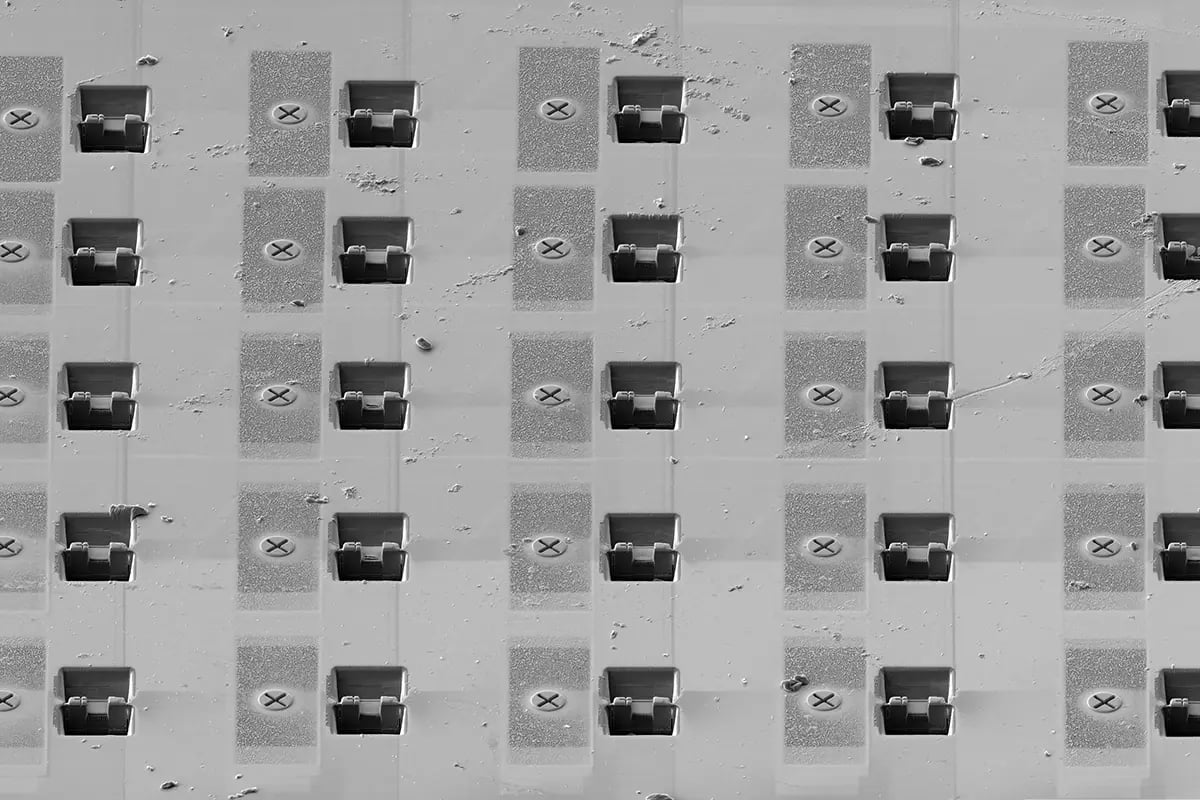
Achieve reproducible cross-sections and 3D reconstructions without curtaining or artifacts. Tescan plasma and Ga+ FIB-SEM workflows deliver smooth surfaces, large-area polishing, and automated slice-and-view tomography.
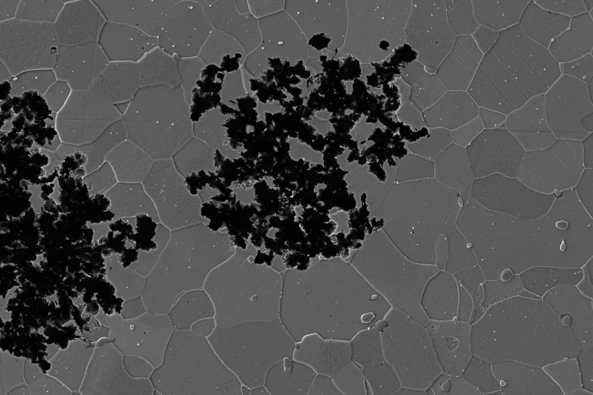
TRUE X-sectioning and Rocking Stage technology ensure reliable EBSD, EDS, and phase mapping results, while high-throughput plasma FIB enables statistically relevant volume analysis.
Generate consistent structural insights that support failure analysis, porosity studies, and large-scale microstructural evaluation with confidence.


.webp?width=1074&height=744&name=VEGA%20LM%20Mat%20Science%20(1).webp)

.webp?width=1086&height=942&name=AMBER-X-TOF%20(2).webp)
