Nanocharacterization Across Broad Variety of Samples
The field-free UHR-SEM column ensures charge-free imaging and analysis optimized for different sample types, including non-conductive, ferromagnetic, or semiconductor devices.
Advanced FIB-SEM for Automated Sample Preparation, Nanoscale Characterization and Nanoprototyping

Tescan AMBER™ 2 is a fully automated Ga⁺ FIB-SEM designed for routine TEM sample preparation, nanoscale characterization, and prototyping across a wide range of materials.
Combining precision with ease of use, it delivers high-quality FIB imaging even at low accelerating voltages. The Field Free BrightBeam™ SEM column ensures nanoscale resolution and exceptional sample analysis versatility.

Understand microstructure, surface detail, and nanoscale behavior with workflows built for precise TEM preparation and confident nanoscale analysis.
AMBER™ 2 gives materials scientists dependable preparation and clear nanoscale insight. Its field-free UHR-SEM reveals fine surface details, while the Ga⁺ FIB new Orage™ 2 enables the most precise and highest quality TEM specimen preparation, especially when combined with AURA™ Gentle Ion Beam. Whether you’re studying microstructure, defects, or preparing TEM samples, AMBER™ 2 supports efficient, confident workflows.
.png?width=951&height=954&name=Aura%20GIB%20Tem%20prep%20(1).png)
Tescan AMBER™ 2 equipped with the Nanoprototyping Toolbox delivers complete FIB-SEM capabilities for nanoscale device prototyping — from design to inspection — empowering users to create, modify, and analyse functional structures without leaving the system.
Design and fabricate novel 2D/3D structures using both electron and ion beam — from plasmonic sensors to freestanding nanowires
Mill, etch, and deposit materials at the nanoscale with precise ion beam control for rapid device prototyping
Unlock new direct fabrication methods for your research — from nanowire-based sensors to 3D magnetic nanodevices and precision surface engineering — with integrated FEBIP and FIBIP processes
Accelerate prototyping cycles from weeks to hours by cross-sectioning and analysing your fabricated devices in-situ — optimise geometry, dose, and material properties without changing tools
Automate even complex prototyping routines end-to-end with Python API and block-based automation — no programming expertise required
Tescan AMBER™ 2 extends nanoscale research capabilities with a fully integrated FIB-SEM environment for fabrication and analysis — one microscope, one software, total control. Researchers and engineers can design, prototype, modify, and characterise nanostructures within one system, maintaining full control over resolution, geometry, and workflow. Whether you're building 3D nanoarchitectures, preparing nanowire devices, or exploring ion implantation for quantum research, AMBER™ 2 supports fast, flexible, and fully controlled nanoscale innovation.


Prepare reliable TEM samples automatically from the most common devices and thin films—on one platform built for fast, predictable semiconductor Lab workflows.
AMBER™ 2 helps semiconductors lab FA lab engineers work with confidence. Its fully automated TEM preparation and range of modalities help R&D Laboratories to investigate new materials and defects in layers stacks with ease.


Resolve cellular structures, delicate interfaces, and complex biological architecture with a platform built for both ambient and cryogenic workflows.
AMBER™ 2 gives life scientists a unified platform for detailed biological imaging. You can move from low-kV surface analysis to correlative cryo-FIB-SEM or cryo-TEM lamella preparation without changing systems, preserving sample integrity while uncovering structure at the cellular and subcellular scale.

Understand microstructure, surface detail, and nanoscale behavior with workflows built for precise TEM preparation and confident nanoscale analysis.
AMBER 2 gives materials scientists dependable preparation and clear nanoscale insight. Its field-free UHR-SEM reveals fine surface detail, while the Ga⁺ FIB enables pthe most precise and highest quality TEM specimen preparation. Whether you’re studying microstructure, defects, or preparing TEM samples, AMBER 2 supports efficient, confident workflows.
.png?width=200&height=200&name=_%20Application%20area%20icon%20(1).png)
Resolve cellular structures, delicate interfaces, and complex biological architecture with a platform built for both ambient and cryogenic workflows.
AMBER 2 gives life scientists a unified platform for detailed biological imaging. You can move from low-kV surface analysis to correlative cryo-FIB-SEM or cryo-TEM lamella preparation without changing systems, preserving sample integrity while uncovering structure at the cellular and subcellular scale.
Precise fabrication and characterization for advanced nanostructures
Tescan AMBER 2 extends nanoscale research capabilities with an integrated environment for fabrication and analysis. Researchers can design, prototype, and characterize nanostructures within one system, maintaining full control over resolution, geometry, and data correlation for advanced nanotechnology applications.
.png?width=201&height=200&name=_%20Application%20area%20icon%20(3).png)
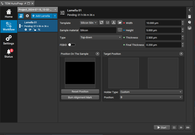
Tescan AMBER™ 2 works seamlessly with Tescan TEM AutoPrep Pro™ to enable fully automated, reproducible TEM lamella preparation. The system manages site selection, trenching, thinning, and polishing with minimal operator input. It produces consistently thin samples while maximizing instrument time efficiency.
TEM AutoPrep Pro™ combines precision automation with real-time imaging through Tescan Essence™ software, ensuring accuracy and repeatability. Together with AMBER™ 2’s BrightBeam™ SEM and Orage™ FIB technologies, this workflow reduces beam exposure, shortens preparation time, and preserves sample integrity for reliable daily operation.