
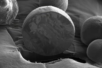
In advanced semiconductor packaging, the primary challenge is often not defect detection itself but efficiently reaching buried regions of interest without introducing preparation-induced artifacts. As packages become increasingly heterogeneous and vertically integrated, failure analysis workflows must balance localization accuracy, preparation speed, and preservation of device integrity across multiple analytical instruments.
That is where the combination of Micro-CT, ultrafast laser processing, and FIB-SEM (Focus Ion Beam - Scanning Electron Microscopy) becomes especially valuable.
-
Micro-CT provides non-destructive insight into buried structures, and its 3D data can serve as a navigational map for identifying the region of interest (ROI).
-
Laser processing enables fast targeted access to such ROIs, but should do so without inducing damage.
-
FIB-SEM delivers the final precision milling, imaging, and analytical investigation needed for detailed investigation.
When integrated into a coordinated workflow, these technologies reduce rework, shorten time-to-data, and improve the repeatability and reliability of advanced failure analysis.
Why disconnected workflows slow failure analysis down
Advanced packages rarely fail in simple, exposed locations. Defects can sit under solder joints, inside stacked dies, around TSVs, or within interfaces surrounded by metals, polymers, and dielectrics.
A disconnected workflow often forces engineers to repeatedly relocate buried features across multiple instruments, increasing preparation time and the risk of damaging sensitive structures.
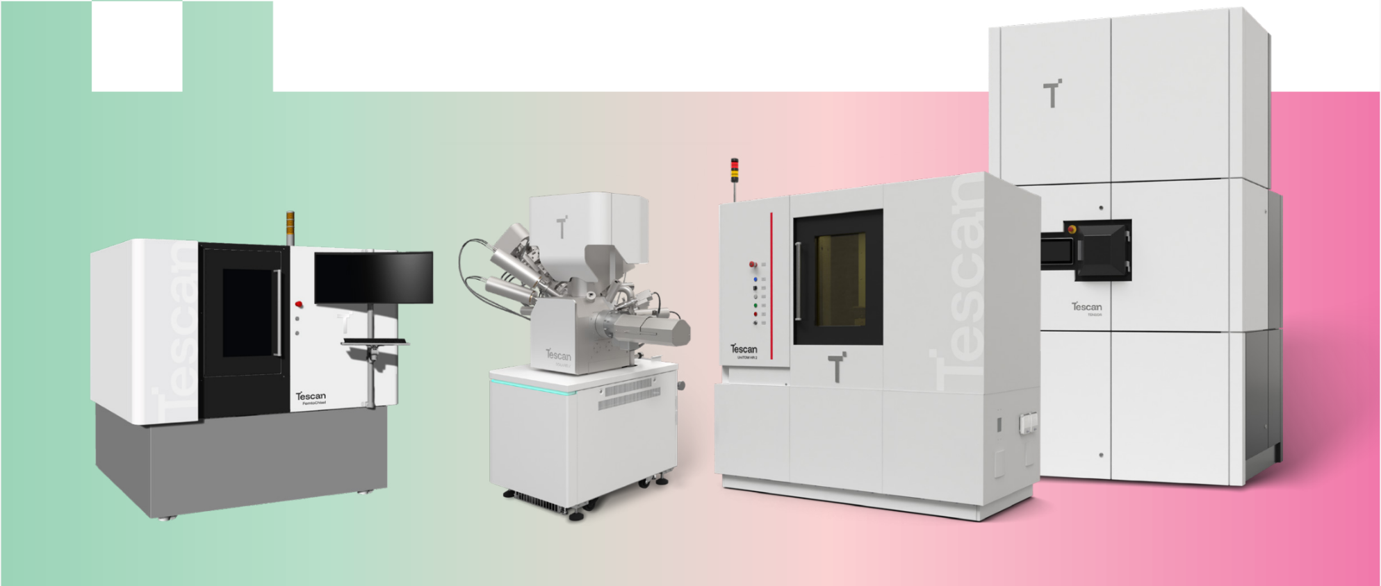
A more integrated approach combines non-destructive volumetric localization, rapid targeted material removal, and nanoscale finishing into a coordinated workflow with shared spatial context between tools
Disconnected workflows create more than just delays; they increase the risk of preparation-induced uncertainty. Early-stage sample alteration, redeposition, or thermal damage can obscure the original failure mechanism and reduce confidence in the final analysis.
Modern failure analysis, therefore, depends on workflows that maintain sample integrity while efficiently transitioning from non-destructive localization to targeted preparation and nanoscale inspection.
Start with non-destructive localization using Micro-CT
Micro-CT enables non-destructive volumetric inspection prior to destructive preparation, helping teams identify buried structures such as solder voids, TSV defects, delamination regions, and interconnect failures. Although spatial resolution and material contrast can vary depending on package composition and size, 3D CT data provide valuable navigation context that reduces destructive trial-and-error during downstream preparation.
Tescan’s semiconductor workflows use Micro-CT for full-device 3D imaging followed by targeted zooms, making it possible to inspect internal structures in their true state. That makes it easier to understand where to cut, where to avoid, and how to preserve the region that matters most.
This step is especially important in advanced packaging, where the ROI may be buried several layers below the surface. A non-destructive overview reduces guesswork and gives the rest of the workflow a clear starting point. Instead of preparing broadly and hoping to land on the right feature, the team can move forward with a more informed access strategy.
Use ultrafast laser processing for fast targeted access
Once the target is known, the next challenge is access.
FemtoChisel is designed for this step.
It operates in the non-thermal ablation regime and is built to reach deeply buried regions of interest without microcracks, melt zones, or redeposition, while delivering reproducible, analysis-ready results across advanced semiconductor devices.
What makes that especially relevant for advanced packaging is the combination of speed and surface integrity. FemtoChisel uses intelligent multi-gas processing and a removable laser protective layer to support cleaner ablation, reduce redeposition, and preserve device integrity across heterogeneous stacks that include metals, polymers, and other packaging materials. In practical terms, that means the laser step can prepare access faster while reducing the cleanup burden that would otherwise fall on the FIB-SEM.
FemtoChisel’s correlative machine vision and in-process depth monitoring further strengthen this step. FemtoChisel can use CT, SEM, or optical data for navigation and targeting, while its integrated nanometer-resolution confocal height sensor supports endpoint precision during processing.
Finish with FIB-SEM where nanometer precision matters most
FIB-SEM remains essential for the final stage of failure analysis. It provides the precise milling, polishing, and imaging needed to resolve structures at the nanoscale and to prepare high-quality cross-sections or lamellae for further analysis. Beyond high-resolution imaging and precision milling, modern FIB-SEM systems can also integrate a wide range of analytical techniques that provide deeper material and structural insight at the nanoscale. Energy-dispersive X-ray spectroscopy (EDS) enables elemental analysis and compositional mapping, electron backscatter diffraction (EBSD) provides crystallographic and grain orientation information, and time-of-flight secondary ion mass spectrometry (TOF-SIMS) supports highly sensitive chemical and molecular characterization. When combined within a single workflow, these analytical capabilities allow failure analysis teams not only to expose buried structures with nanometer-scale precision, but also to correlate morphology, composition, crystallography, and chemistry within the same region of interest. This multi-modal analytical approach is increasingly important in advanced semiconductor packaging, where failures often involve complex interactions between materials, interfaces, and processing conditions.
Tescan FIB-SEM systems combine high-resolution SEM imaging with precise ion beam milling to support both structural characterization and advanced analytical workflows. Depending on the application, users may select Ga FIB for high-precision nanoscale work or Xe plasma FIB for faster large-volume material removal, allowing the workflow to be optimized for either ultimate precision, throughput, or a balance of both.
In advanced packaging workflows, this level of precision is what transforms physical access into meaningful analytical insight. Clean cross-sections and site-specific preparation across structures such as BGAs, TSVs, MEMS, and OLED devices enable more accurate root-cause analysis while minimizing preparation-induced artifacts. By incorporating FemtoChisel upstream for rapid bulk access, the FIB-SEM can focus less on large-volume material removal and recovery steps, and more on the high-resolution imaging, precision polishing, and analytical characterization needed to fully understand the failure mechanism.
Why the integrated workflow matters
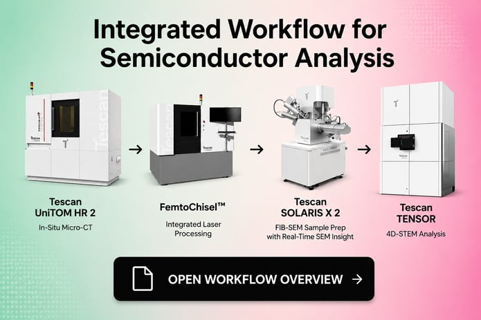
The strength of this workflow is not just that each tool performs well on its own. It is that each tool handles the part of the job it is best suited for. Micro-CT localizes the problem non-destructively. FemtoChisel opens access quickly and cleanly. FIB-SEM completes the final preparation and analysis with nanometer-scale control. Together, they reduce the friction between steps and make the overall process more efficient and more reliable.
For industry teams working under pressure to improve throughput, reduce rework, and preserve device integrity, that shift is significant. The workflow becomes less about recovering from artifacts and more about reaching the answer faster, with greater confidence in the result.
Conclusion
Failure analysis in advanced packaging is no longer just a question of imaging power. It is a question of workflow design. By combining non-destructive Micro-CT, clean ultrafast laser access, and precise FIB-SEM finishing, semiconductor teams can move more efficiently from buried defect localization to final root-cause analysis. That is what makes an integrated workflow so valuable: it shortens the path from problem to insight without sacrificing sample quality along the way.
The future of semiconductor failure analysis will be defined by integrated workflows that combine speed, precision, and multi-modal analytical capability across multiple length scales. Tescan’s unique strength is its ability to unify these capabilities-from non-destructive X-ray imaging and ultrafast laser processing to FIB-SEM nanomachining and advanced analytical characterization-into a single coordinated workflow.
By minimizing preparation-induced artifacts such as redeposition, thermal damage, and unintended sample alteration, the Tescan workflow helps preserve device integrity throughout the analysis process, increasing confidence in the final root-cause determination. At the same time, reducing preparation bottlenecks and workflow fragmentation enables semiconductor engineers to move more efficiently from buried defect localization to high-resolution analytical insight in increasingly complex advanced packaging environments.
Explore the integrated workflow overview
Explore how Micro-CT, laser processing, FIB-SEM, and 4D-STEM connect within advanced semiconductor analysis workflows.
Q&A
Why start failure analysis with Micro-CT?
Micro-CT provides non-destructive 3D inspection of complex packages and allows targeted zooms into internal structures, helping teams localize buried defects before destructive preparation begins.
What does FemtoChisel add to this workflow?
FemtoChisel provides rapid targeted access to buried regions of interest while minimizing thermal damage, redeposition, and other preparation-induced artifacts that can compromise downstream analysis. Compared to conventional mechanical preparation methods, ultrafast laser processing can remove material significantly faster across complex heterogeneous stacks while reducing the risk of smearing, cracking, or mechanically altering delicate structures.
Compared to relying on FIB-SEM alone for large-volume material removal, FemtoChisel dramatically reduces the amount of bulk milling required inside the FIB, allowing the FIB-SEM to focus on final high-precision polishing, imaging, and analytical characterization rather than time-consuming excavation. This not only improves throughput, but also increases confidence in the final root-cause analysis by preserving device integrity throughout the workflow.
Why is FIB-SEM still necessary?
FIB-SEM remains the critical final step in advanced semiconductor failure analysis because it provides the nanometer-scale precision needed for final cross-sectioning, polishing, imaging, and site-specific sample preparation. While upstream tools such as Micro-CT and FemtoChisel help localize defects and rapidly expose buried structures, FIB-SEM enables the detailed structural and material analysis required to fully understand the failure mechanism.
Beyond precision milling and high-resolution SEM imaging, Tescan FIB-SEM systems also support a wide range of integrated analytical techniques. EDS enables elemental mapping and compositional analysis, EBSD provides crystallographic and grain orientation information, and TOF-SIMS delivers highly sensitive chemical and molecular characterization. Together, these capabilities allow engineers to correlate structural, compositional, crystallographic, and chemical information within the same nanoscale region of interest.
By using FemtoChisel upstream for rapid bulk material removal, the FIB-SEM can focus less on time-consuming excavation and more on the high-value analytical work that ultimately drives accurate root-cause analysis.
Which semiconductor applications benefit most from this approach?
This integrated workflow is especially valuable for semiconductor applications that involve complex multilayer structures, buried regions of interest, and high-value devices where preparation-induced artifacts can compromise the final analysis. It is particularly well suited for advanced packaging failure analysis, including BGAs, TSVs, chiplets, heterogeneous integration, 2.5D/3D packages, wafer-level packaging, and hybrid bonding structures.
The workflow is also highly beneficial for buried defect localization, delayering and reverse engineering, TEM lamella preparation, process development, and materials characterization workflows that require precise correlation between structural, compositional, and crystallographic information.
By combining non-destructive Micro-CT localization, rapid ultrafast laser access, and high-resolution FIB-SEM analysis with integrated analytical techniques such as EDS, EBSD, and TOF-SIMS, the workflow enables faster and more reliable root-cause analysis while minimizing preparation-induced damage and reducing overall time-to-insight.
Written by Sina Shahbazmohamadi
Head of Technology, Laser Technologies Business Unit, Tescan


FemtoChisel™: Redefining Ultrafast Laser Processing
On-demand Webinar