.jpeg?width=352&name=Image%20(99).jpeg)
ISTFA 2026 once again served as a leading platform for semiconductor failure analysis professionals to exchange knowledge, share emerging methodologies, and discuss the challenges presented by advanced packaging and increasingly complex semiconductor devices.
Throughout the conference, Tescan engaged with engineers, researchers, and industry experts to explore how integrated workflows and automation can help streamline failure analysis processes, improve throughput, and accelerate insight generation.
An End-to-End Semiconductor Failure Analysis Workflow
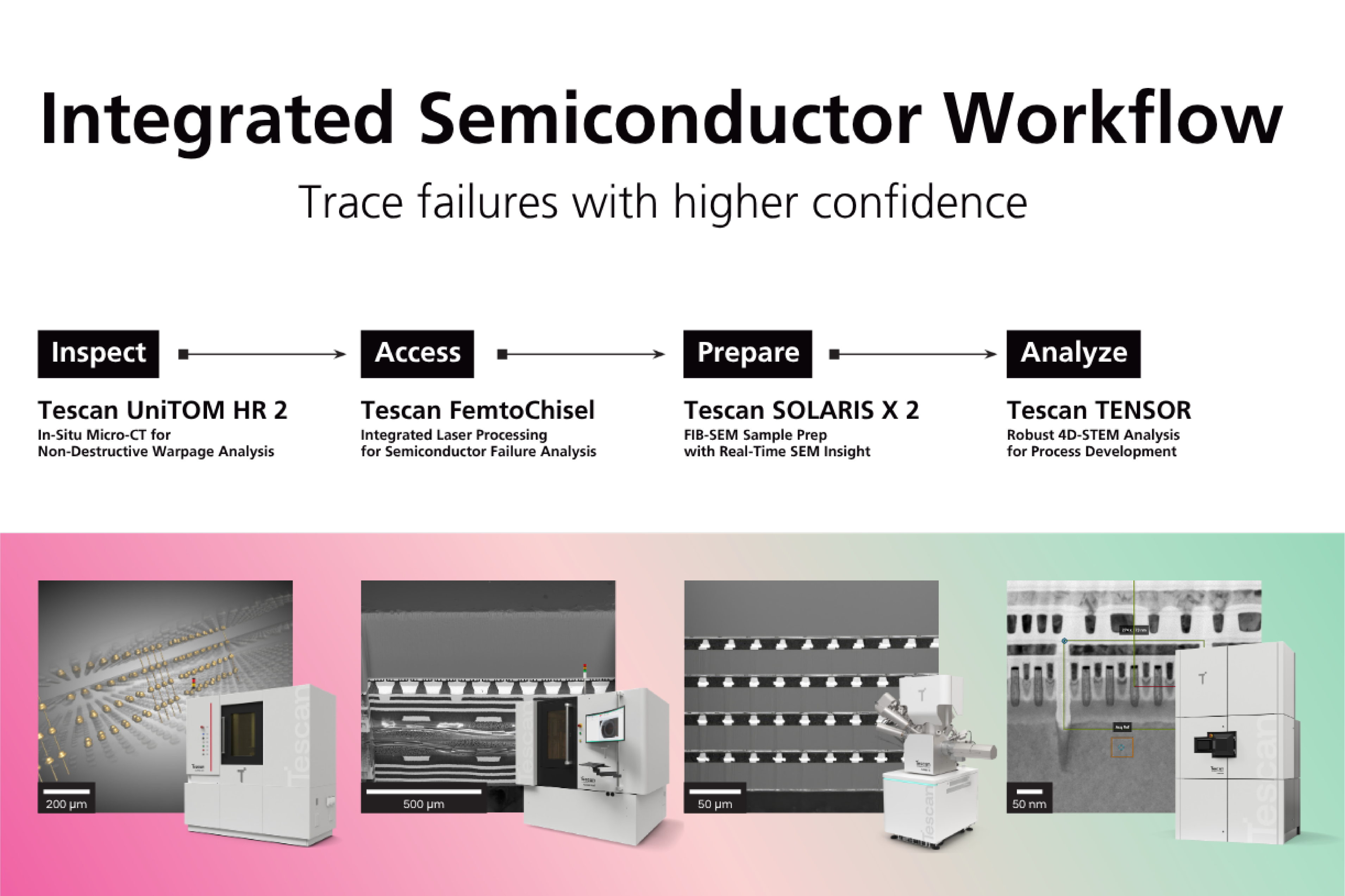
At Booth 605, Tescan demonstrated its semiconductor failure analysis workflow built around four connected stages:
Inspect → Access → Prepare → Analyze
The workflow illustrates how complementary technologies can be combined to support the full failure analysis process, from initial non-destructive inspection through targeted sample preparation and detailed characterization.
By connecting each stage of the workflow, engineers can more efficiently identify areas of interest, access buried structures, prepare high-quality samples, and perform the analyses required to understand device failures or process-related issues.
.jpeg?width=1200&length=1200&name=Image%20(97).jpeg)
Industry Conversations Focused on Efficiency and Automation
Many discussions at ISTFA reflected the challenges facing semiconductor failure analysis teams as device architectures continue to increase in complexity. Conversations frequently focused on electrical and physical fault isolation, device delayering, SEM imaging, TEM sample preparation, and the need for higher-throughput analysis workflows.
A recurring theme throughout the event was the growing interest in artificial intelligence and automation. Attendees were particularly interested in how AI-assisted workflows can help reduce analysis time, improve defect localization, and support more consistent decision-making. Significant interest was also shown in FemtoChisel™, with many visitors highlighting its potential to accelerate sample preparation and fault isolation processes.
Discussions around Tescan TENSOR™ further demonstrated the industry's focus on advanced analytical approaches for semiconductor failure analysis applications and next-generation semiconductor devices.
Technical Presentation: AI-Driven Failure Analysis Workflows
From Access to Insight: An AI-Based End-to-End Failure Analysis Pipeline Combining Laser Sample Prep, Correlative Navigation, and Automated Image Analytics
Presented by Dr. Pouya Tavousi
Dr. Tavousi highlighted an AI-enabled workflow that integrates laser sample preparation, correlative navigation, and automated image analytics to streamline defect localization and accelerate the path from physical access to actionable insight.
The approach demonstrated how automation can help address growing workflow complexity while supporting faster and more reliable failure analysis outcomes.
Poster Session Contributions
High-Throughput Laser Sample Preparation & Device De-processing
Presented by Dave Zapotok
This poster focused on laser-based sample preparation and device de-processing workflows designed to support higher throughput and improved efficiency in semiconductor failure analysis.
The work highlighted approaches that can help reduce preparation times while maintaining the sample quality required for downstream characterization.
STEM Nanobeam Diffraction for Strain Analysis at Sub-2 nm Resolution
Presented by Dr. Daniel Němeček
This poster demonstrated advanced 4D-STEM strain analysis enhanced by integrated electron beam precession, enabling strain characterization at sub-2 nm spatial resolution.
The workflow combines high spatial resolution with high-throughput characterization capabilities, making routine, high-precision strain measurements more accessible for semiconductor failure analysis and process development applications.


Looking Ahead
ISTFA 2026 reinforced the industry's continued focus on workflow integration, automation, and analytical precision. As semiconductor devices become increasingly complex, failure analysis teams require solutions that connect multiple stages of the workflow while maintaining speed, accuracy, and reproducibility.
From AI-assisted defect localization and laser-based sample preparation to advanced microscopy and characterization techniques, Tescan's participation highlighted the value of bringing these capabilities together in a connected workflow that helps engineers move more efficiently from inspection to insight.
We thank everyone who visited Booth 605, attended the presentation sessions, and contributed to the many technical discussions throughout the event. The conversations at ISTFA continue to provide valuable perspectives on the evolving needs of the semiconductor failure analysis community.


Related Resources
FemtoChisel™ Laser Processing
Explore ultrafast laser processing for sample preparation.

4D-STEM in SEM
Discover advanced nanoscale analysis using 4D-STEM.

Advanced Packaging Failure Analysis
Explore correlative Micro-CT and FIB-SEM workflows.