Achieve Non-Destructive Failure Analysis with Tescan Micro-CT 


Use high-resolution micro-CT to scan devices and components without disassembly. Visualize internal structures in real time with clear material contrast for confident analysis.

Non-Destructive_Failure_Analysis_with_Micro-ct

Tescan solutions

for advanced research in semiconductors
Micro-CT for Electronics: Fast, Non-Destructive 3D Imaging
Use Tescan UniTOM Micro-CT systems to perform non-destructive 3D visualization of consumer electronics,  from full device to individual components.
 
  • Overcome Teardown Challenges with Micro-CT for Consumer Electronics Inspection

    • Disassembly carries the risk of damaging fragile parts or changing the internal structure and may not provide true 3D context or enable access to components embedded deep inside.  

  • Why Using Micro-CT for Non-Destructive Testing of Consumer Electronics Makes Sense

    • Inspect full devices and zoom in to component-level defects
    • Expose internal battery faults without breaking the seal
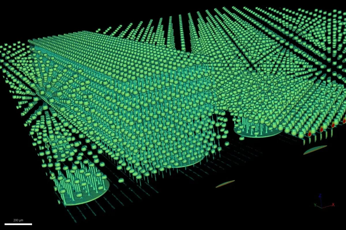
    • Verify TSV alignment with submicron VOI scans
    • Reveal hidden voids in BGA solder bumps
    • Inspect wire bonds in microchips with high resolution
Semi 4- HBM_1x

Tescan Solutions

for Consumer Electronics

Tescan UniTOM HR

TESCAN UniTOM HR delivers high-resolution and dynamic micro-CT for component-level testing. Fast image processing and precision imaging make it ideal for small samples, while true 4D capabilities capture structural changes in real time.

  • True 4D dynamic CT: Provides sub-5-second temporal resolution
  • High spatial resolution: Resolves features below 600 nm
  • In-situ compatibility: Supports rotational stages, pressure setups, and powered devices
MICRO_UniTOM_HR_1-2

 Tescan UniTOM XL  

TESCAN UniTOM XL delivers versatile micro-CT inspection for full devices and large assemblies. A large scanning envelope and powerful X-ray source let you capture both fast overviews and detailed zooms in a single system.

  • Dual-scan capability: Delivers quick overviews and high-resolution detail in one workflow
  • Large-sample capacity: Accommodates devices up to 45 kg and 1000 mm wide
  • Adjustable geometry: Offers flexible source-to-detector distance for optimal resolution on large parts
MICRO_UniTOM_XL_1-2

Sign up for a personal virtual demo

Our global team is available to answer questions about Tescan solutions for Semiconductors.

GET IN Touch

Contact us

map

Where can you find us:

Tescan Brno
Libušina třída 21
623 00 Brno
Czech Republic

info@Tescan.com