
Back to the webinars

WEBINAR | Your TEM lamella is thin. So why isn't the image as good as you want?


A hands-on FIB-SEM workflow for reducing preparation artifacts before high-resolution TEM analysis 

Dec 2, 2026

Morning: 9:00 CEST / 3:00 EDT / 12:00 PDT

Afternoon: 19:00 CEST / 13:00 EDT / 10:00 PDT

You prepared the lamella, reached the target thickness and transferred it successfully. But in the TEM, interfaces still look blurred or the analytical signal is difficult to interpret.

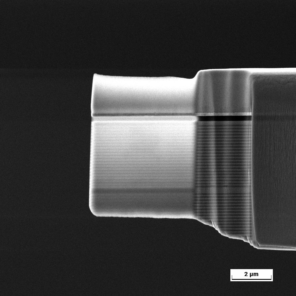
In this hands-on session, Tescan application specialists will work through a real TEM specimen-preparation workflow and show where preparation artifacts can be introduced. You will see how to recognize common issues associated with final Ga⁺ FIB thinning, how to select a suitable finishing strategy and how integrated low-energy Ar⁺ polishing with Tescan AURA™ can help remove the affected surface layer before the specimen leaves the FIB-SEM.

The focus will be on practical decisions you can apply in the lab: how to do final thinning properly, what parameters matter and how to check whether the lamella is ready for high-resolution imaging and analysis. 

What attendees will learn

  • Why a lamella can be electron-transparent but still unsuitable for high-resolution TEM

  • How to recognize Ga implantation, redeposition and other preparation-related effects

  • When low-kV Ga⁺ finishing may be sufficient and when Ar⁺ polishing should be considered

  • How to select a polishing strategy for different materials and specimen geometry

  • How to inspect the lamella before transferring it to TEM 

Register for this hands-on webinar to learn how to reduce preparation artifacts, optimize final thinning, and improve TEM specimen quality using FIB-SEM and AURA™ polishing.


Speakers

maksym
Maksym Klymov

Head of Applications Department, Tescan


Maksym leads Tescan’s Applications and Demo Labs team, supporting the development and practical use of advanced electron microscopy workflows. His experience spans SEM, FIB-SEM, sample preparation and materials characterization, with a strong focus on translating instrument capabilities into reliable workflows that address real laboratory challenges.
 

jan roncak
Jan Roncak, PhD

Application Specialist, Tescan


Jan is a materials science application specialist at Tescan, focusing on FIB-SEM workflows and advanced sample preparation. With a research background in materials engineering and electron-beam processing of complex alloys, he brings a practical understanding of how preparation conditions affect microstructure and the reliability of the final microscopy results. 

Don't miss out - register now.


Register for the webinar