Semiconductor Failure Analysis Workflows
Explore how Tescan connects non-destructive inspection, targeted access, sample preparation and high-resolution analysis for advanced packaging and failure analysis challenges.

Explore how Tescan connects non-destructive inspection, targeted access, sample preparation and high-resolution analysis for advanced packaging and failure analysis challenges.

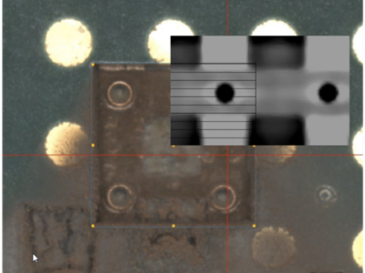
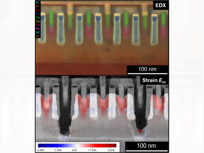
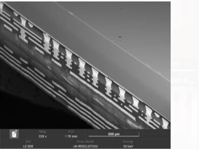
Discover application images, videos and real examples showing what Tescan technologies can reveal, access and prepare, including deeply buried regions and complex material stacks.

Learn about the latest developments across Tescan’s semiconductor workflow, from defect localisation and laser-enabled access to FIB-SEM preparation and downstream analysis.

Bring your failure-analysis or packaging question to the booth. Our semiconductor application experts are ready to discuss your sample, workflow bottlenecks and possible next steps.
12:45 - 13:45
February 27, 2023
12:45 - 13:45
February 27, 2023
12:45 - 13:45
February 27, 2023
12:45 - 13:45
February 27, 2023
12:45 - 13:45
February 27, 2023
12:45 - 13:45
February 27, 2023
February 27, 12:45 - 13:45, LL Copernicum, level 0
February 27, 12:45 - 13:45, LL Copernicum, level 0
February 27, 12:45 - 13:45, LL Copernicum, level 0
February 27, 12:45 - 13:45, LL Copernicum, level 0
February 27, 12:45 - 13:45, LL Copernicum, level 0
February 27, 12:45 - 13:45, LL Copernicum, level 0
12:45 PM - 01:45 PM
February 27, 2023
February 27, 12:45 PM - 01:45 PM, booth 123
Introducing MIRA XR – the analytical SEM reimagined for speed, usability, and ultra-high-resolution imaging. Perfect for analytical workflows across materials science disciplines. Designed to deliver high throughput without compromising on resolution or automation. A productivity platform for every user, from QA labs to advanced research teams.
Located at TESCAN's Booth 1324
Register for a short in-booth session.
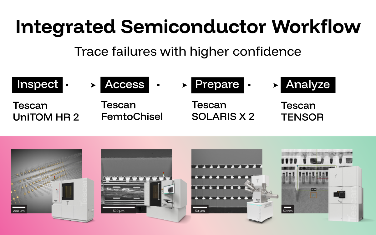
VISUALIZE → ACCESS → PREPARE → ANALYZE
One connected workflow from buried defect to root cause determination.
You can Book a Demo directly at Tescan Booth 605.
15:20 - 15:40
October 6, 2026

15:00 - 16:00
October 7, 2026

15:00 - 16:00
October 7, 2026
October 6, 15:20 - 15:40, Bridge Hall
October 7, 15:00 - 16:00, Exhibit Hall
October 7, 15:00 - 16:00, Exhibit Hall
Semiconductor Business Development (Global)
Semiconductor Product Marketing
Semiconductor Business Development (North America)

FIB-SEM Business Development (North America)
Head of AI and Advanced Solutions - Laser Solutions
Product Sales Lead - Laser Solutions
Product Sales Lead - STEM Solutions
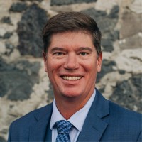
Vice-President of Sales (Americas)
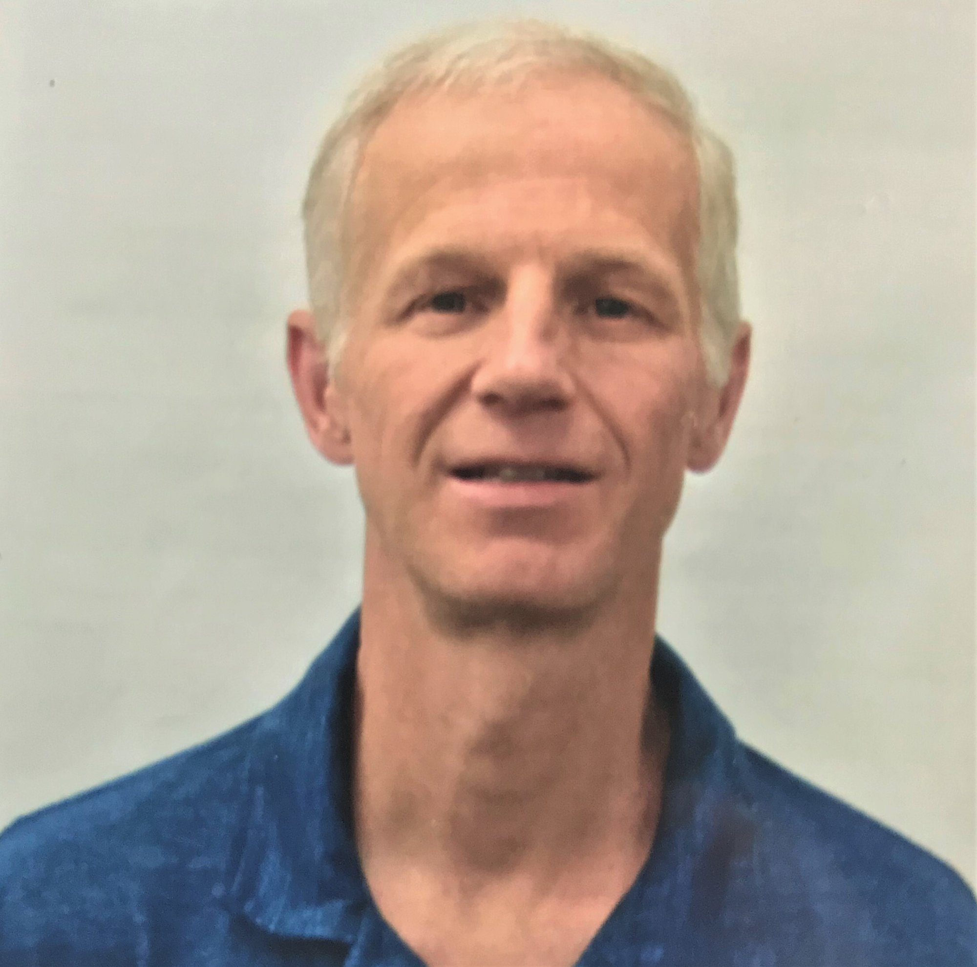
Sales Manager (US Northwest)
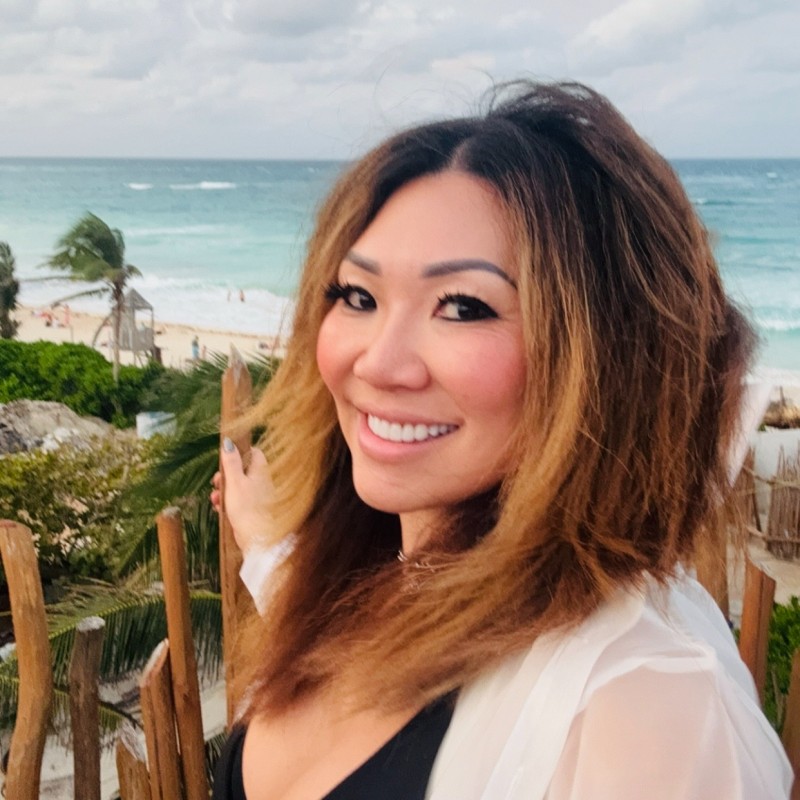
Sales Manager (US Southwest)
Area Sales Director (Singapore)
Area Sales Director (US West & South America)