
Automation improves throughput and makes TEM sample prep more accessible, but high-resolution (S)TEM still depends on sample quality. A lamella can be thin and still contain damage or artefacts that affect the final data.
Listen to article
If you work with FIB-SEMs, you have likely noticed that automation has become a major focus for instrument manufacturers. This blog post is not an argument against that shift. Automated TEM workflows are essential to an efficient laboratory: they increase throughput by enabling unattended operation outside working hours and make sample preparation routines more accessible to less experienced operators.
However, a successful TEM or STEM analysis - and the scientific insight it provides - still depends on sample quality. Automated workflows can reliably produce samples thinner than 100 nm and finish them at low accelerating voltages to reduce damage. This level of quality is sufficient for many standard (S)TEM sessions. Lattice imaging and other high-resolution TEM studies, however, demand more. That is why quality must remain the other half of the story.
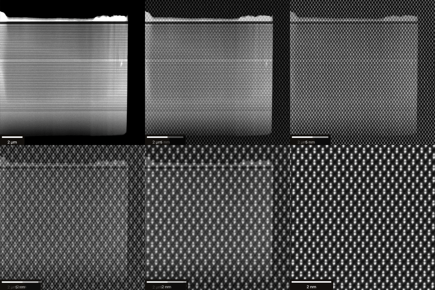
Figure 1. Aura™ polishing at 200 eV reduces FIB damage in sub-50 nm lamellae, including Ga+-sensitive materials, producing 2–3× fewer ion-induced defects than Ga+ finishing.
You may be wondering whether preparing samples for high-resolution (S)TEM can also be made easier- or even automated. Before answering that question, it helps to look at the traditional approaches used in workflows that combine TEM sample preparation with FIB-SEM.
Low-Voltage FIB-SEM Polishing for TEM Sample Preparation
The most common approach is to use the FIB-SEM itself and reduce the accelerating voltage, typically to a minimum of around 500 eV. High-energy ions - up to 30 keV in commercial FIB-SEMs - penetrate deeper into the material and can create structural changes commonly described in the literature as amorphous damage [1]. Reducing the ion energy decreases the penetration depth and therefore limits damage at the TEM sample surface.
Penetration depth also depends on the size and mass of the ion species. Heavier ions generally dissipate their energy closer to the surface and do not penetrate as deeply as lighter ions. The workflow may therefore look like the one shown in Figure 2. At a high accelerating voltage, the sample is first thinned to approximately 100 nm. When a Ga+ FIB-SEM is used to polish silicon, roughly half of this thickness may be damaged or amorphized, while about 50 nm of pristine material remains in the center. Applying a lower accelerating voltage then reduces the amorphous layer while helping to preserve the intact material in the center. By lowering the voltage in a controlled way, it is possible to prepare samples with minimal damage and a thickness below 50 nm - or even less.
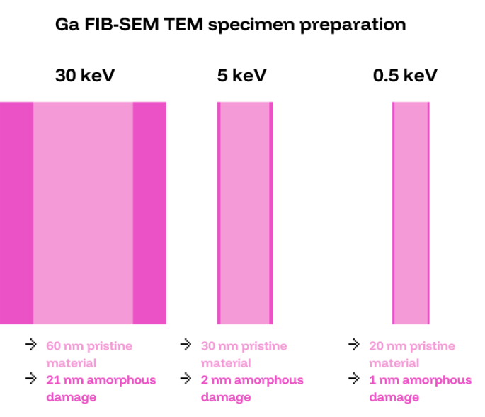
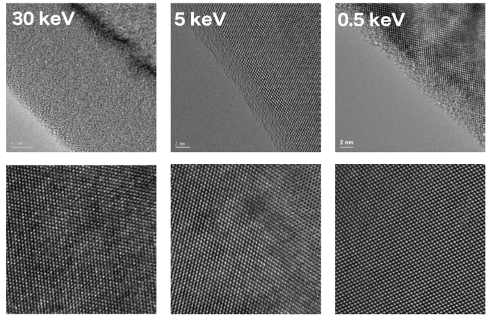
Figure 2. Schematic representation of the TEM sample-thinning workflow. (Top) Remaining pristine material and representative amorphous damage after ion polishing at 30 keV, 5 keV, and 0.5 keV. (Bottom) Representative TEM images showing amorphous damage and sample image quality at the corresponding ion energies.[1]
The limitation is that this approach requires experience and a good understanding of the interaction between the ion beam and the sample.
Stand-Alone Argon Ion Beam Polishing for TEM Lamellae
Another option is to use a separate ion polisher for final thinning and damage reduction after the initial FIB-SEM preparation. These systems operate at low accelerating voltages-sometimes below 500 eV-and use inert ion species such as argon. Unlike conventional Ga+ FIB-SEM finishing, argon polishing does not introduce additional gallium into the specimen. Xenon plasma FIB-SEMs can likewise avoid gallium implantation during the preceding preparation step. Stand-alone argon polishing can further reduce surface damage while continuing to thin the TEM sample, following the same general principle illustrated schematically in Figure 2: lower ion energy reduces the penetration depth and limits damage.
This approach also introduces practical challenges. Transferring a fragile sample from the FIB-SEM holder to a dedicated polishing holder increases the risk of contamination or sample loss. In addition, stand-alone systems do not provide visual process and quality control. Polishing is therefore effectively blind, which places even greater demands on the operator’s experience.
Integrated Gentle Ion Beam Polishing in the FIB-SEM
A third option addresses these limitations by integrating an argon ion polisher directly into the FIB-SEM. The sample remains sealed in the same vacuum chamber and stays on a shared holder, reducing the risk of damage and contamination. Integration also enables visual control through the SEM optics and even allows a STEM detector in the FIB-SEM to capture TEM-like contrast directly during the workflow.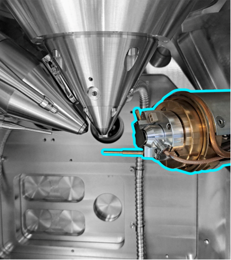 Figure 3. Schematic representation of an argon Gentle Ion Beam polisher integrated into the FIB-SEM workflow, enabling in situ TEM sample polishing.
Automated TEM Lamella Preparation with Integrated Gentle Ion Beam Polishing
Integration also creates opportunities to automate the polishing process further. This makes the workflow less complex and more approachable for users who are new to TEM sample preparation but need high-quality results from the beginning.
The first step is to move the sample from the FIB-SEM position to the argon ion polishing position. This transition is performed automatically, as shown in the attached Video 1.
Video 1. Automated holder reconfiguration from the FIB-SEM TEM sample preparation position to the Aura™ Gentle Ion Beam polishing position as part of the workflow, minimizing the risk of damage to the sample or instrument. The video speed has been increased.
To create a finely polished TEM surface, the sample must be positioned precisely relative to the ion flow. The two broad faces of the lamella are polished in turn, and the sample can alternate between closely spaced angular positions during polishing - a movement known as oscillation - to help prevent artifacts such as curtaining.
Together with the ability to polish at energies as low as 200 eV, these steps can deliver the quality required to make a sample ready for high-resolution (S)TEM. Although the procedure may sound demanding, it can also be automated. The workflow uses presets: the operator can select an existing one, adjust it when necessary, and let the process run. The process for configuring a polishing cycle with the integrated Aura™ Gentle Ion Beam is explained in detail in Video 2.
Visual monitoring remains an important advantage. It allows the operator to assess sample quality throughout the process and adjust the milling conditions as polishing progresses. Sample movement and positioning are handled automatically, helping even novice users prepare high-quality TEM lamellae with greater confidence.
Video 2. Automated polishing with the integrated Aura™ Gentle Ion Beam, showing oscillation and automatic switching between the two sides of the TEM lamella. The video speed has been increased.
Interested in a closer look? Our Demo Bites videos offer a more detailed walkthrough of the workflow, with explanations from our experts.
Story completed: High-Quality Meets Accessibility
We began with the statement that automation is only half the story. This does not make automation any less important: it solves the accessibility challenge. The sample-quality challenge is addressed by the hardware through Gentle Ion Beam polishing with inert argon ions. To keep the workflow truly accessible, this final step must also be integrated and automated.
This is exactly what motivated us to develop this solution: making high-quality TEM sample preparation easier and more accessible. By combining automated FIB-SEM sample preparation with an automated Gentle Ion Beam polishing step, the complete workflow brings both sides of the story together. Integration protects the sample and provides high-resolution visual control throughout the process, while automation makes the workflow approachable for a wider range of users. Together, they deliver the quality that advanced microscopy demands without adding unnecessary complexity.
If you would like to learn more about Aura™ Gentle Ion Beam, explore the product page or request a demonstration directly.
References
[1] Giannuzzi, 2 keV Ga+ FIB Milling for Reducing Amorphous Damage in Silicon, Microscopy and Microanalysis, 11(S2), (2005). doi:10.1017/s1431927605507797



Related Resources
Improve TEM Lamella Quality
Explore AURA™ polishing for better TEM specimens.

AURA™ Gentle Ion Beam
Gentle Ar⁺ polishing for TEM specimens.