Designed for Precise Lamella Quality Assessment 

Integrated Retractable

4D-STEM Detector

for FIB-SEM 

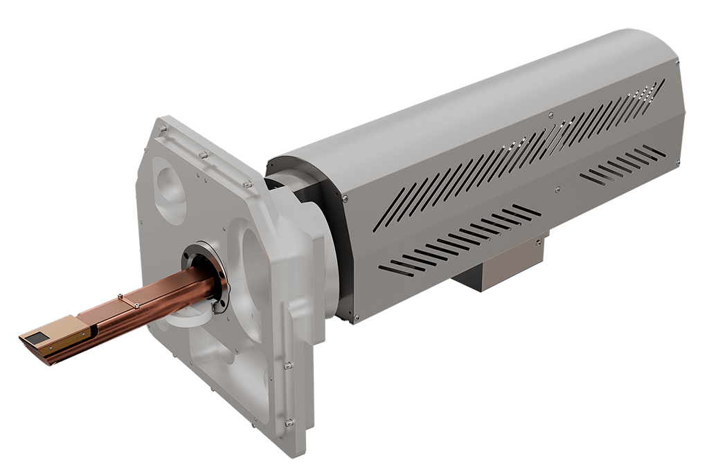
4D STEM detector - hero - desktop
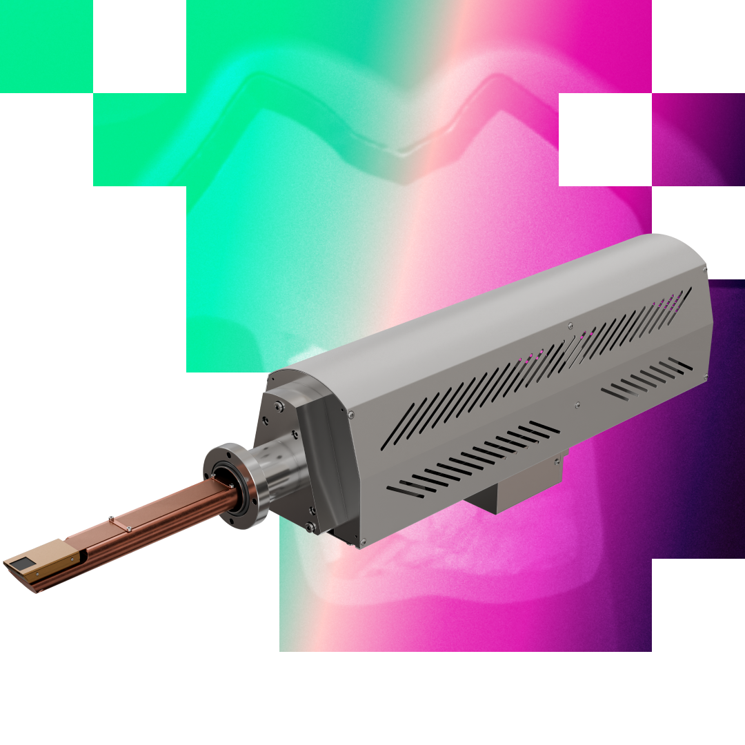
4D STEM detector - hero - mobile

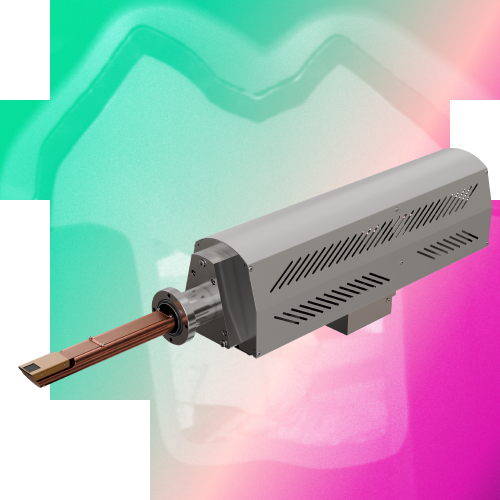
The fully retractable, SEM chamber-integrated 4D-STEM detector enables direct sample and material characterization at ultra-high resolution, as well as fast and precise sample quality pre-screening for materials science applications.

By capturing a diffraction pattern at every scan point, the 4D-STEM detector generates a comprehensive dataset that serves as a rich source of information. Subsequent data processing enables extraction of precise nanoscale crystallographic information, such as crystal orientation, grain structure, and phase transformation. This approach makes material characterization faster and more accessible.

The acquired 4D datasets can be reprocessed multiple times without remeasuring the sample and are fully compatible with open-source software, enabling the development of new, user-defined analysis methodologies.

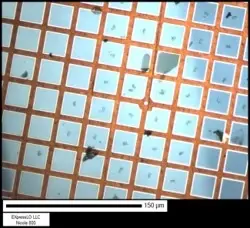
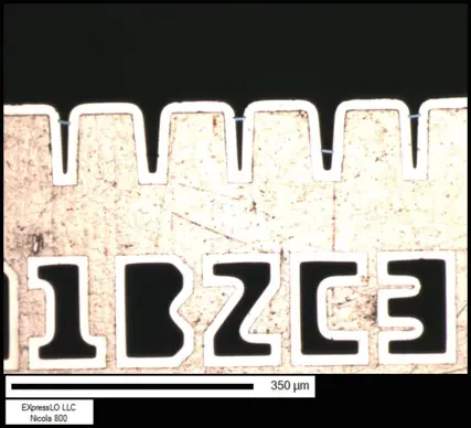
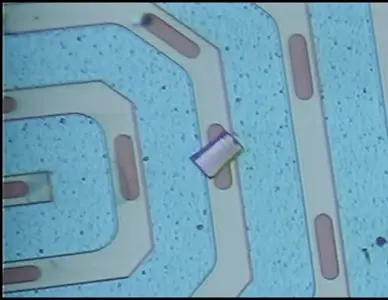
The 4D-STEM detector also allows for immediate evaluation of lamella quality directly inside the FIB-SEM after final FIB polishing, thereby reducing the risk of sample reworking and repeated TEM analysis.

With an integrated 4D-STEM detector, Tescan AMBER™ 2 and Tescan AMBER X™ 2 are robust, high-performance FIB-SEM platforms for advanced materials science workflows. Both systems feature the BrightBeam™ SEM column for ultra-high-resolution imaging and support a full suite of multimodal characterization techniques, including EDS, EBSD, ToF-SIMS, and Raman.

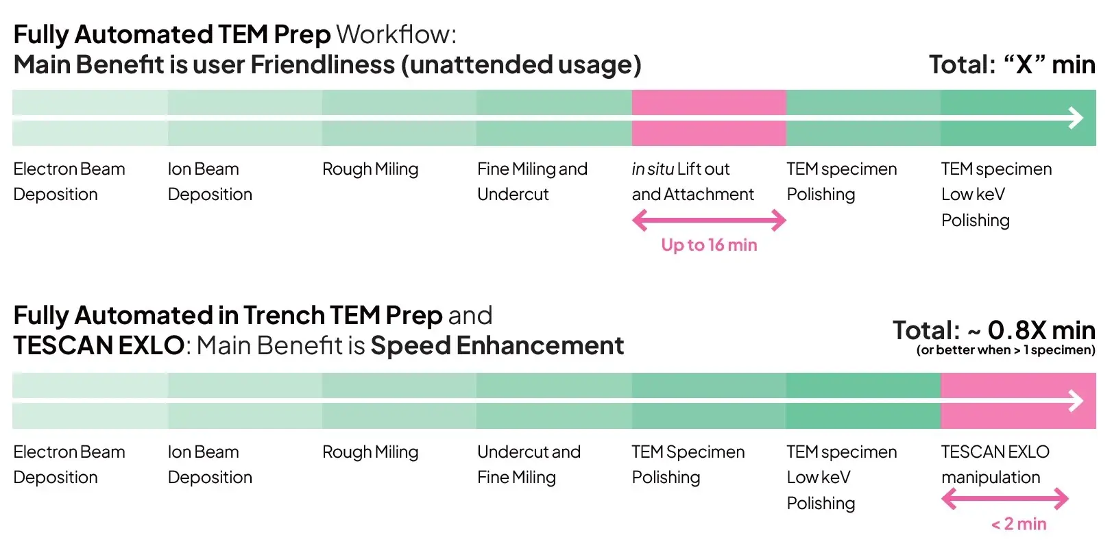
For streamlined and reliable TEM lamella preparation, the platforms leverage advanced automation through TEM AutoPrep™ Pro, while the fully integrated Aura™ Gentle Ion Beam enables final argon polishing for the excellent lamella quality.

AMBER X™ 2 is a versatile solution for fast, Ga+-free, and low-damage specimen preparation. Its Mistral™ xenon plasma FIB source is specifically designed for both precise and routine high-quality sample preparation, along with high-speed milling of large volumes, enabling large-scale 3D multimodal characterization across hard, soft, and beam-sensitive materials.

AMBER™ 2 is designed for high-precision TEM lamella preparation and nanoprototyping. Utilizing the Orage™ 2 Ga FIB column, it delivers the accuracy and surface quality required for the most delicate nanostructuring tasks.

  • Fully retractable, SEM chamber-integrated 4D-STEM detector with beam scan synchronization  

  • Direct quality control and pre-screening of TEM lamellae and air-sensitive samples immediately after FIB preparation within the same instrument  
  • Fast acquisition and high-resolution imaging (<1 nm) for sample evaluation and a broad range of applications  
  • Accelerated material characterization through nanoscale crystallographic insights at every scan point  
  • 4D-STEM datasets enabling repeated analysis, fully compatible with open-source software (e.g., LiberTEM, py4DSTEM, pixStem)
  • Seamless integration into AMBER™ 2 and AMBER X™ 2 platforms for an enhanced TEM lamella preparation workflow  

WHERE RETRACTABLE 4D-STEM DETECTOR MAKES THE DIFFERENCE

Direct TEM lamella quality control

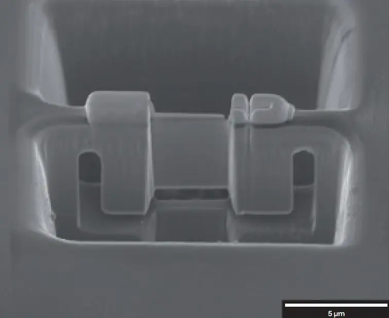
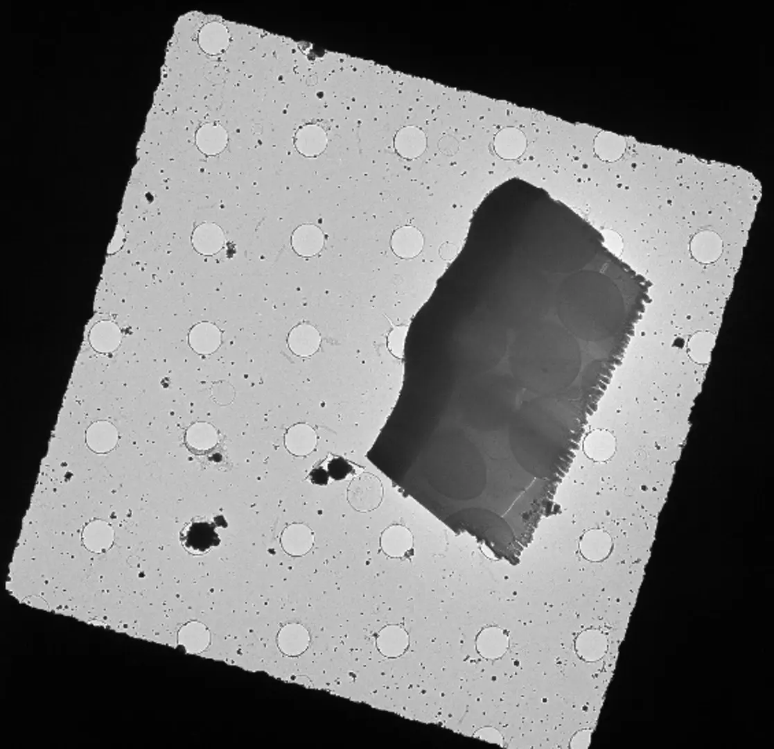
Direct verification of TEM lamella thickness and crystallinity in the FIB-SEM through well-defined diffraction patterns ensures samples are ready for subsequent TEM analysis after final FIB polishing. This significantly reduces failure rates, minimizes rework, and improves overall FIB-SEM-to-TEM workflow efficiency.

Extended analytical capabilities

Direct acquisition of 4D-STEM data within the FIB-SEM enables advanced nanoscale characterization, with post-processing allowing identification of phase composition and crystal orientation, eliminating the need for sample transfer to a dedicated TEM.

Acquired 4D-STEM datasets are fully compatible with open-source analysis applications such as LiberTEM, py4DSTEM, and pixStem and can be reprocessed multiple times. Combined with Expert PI, a scripting and automation environment for FIB-SEM, this approach provides the flexibility to develop new analysis methodologies and create custom data-processing workflows tailored to specific applications.

4DSTEM_live_apertury-800px-2

Flexible imaging contrast selection

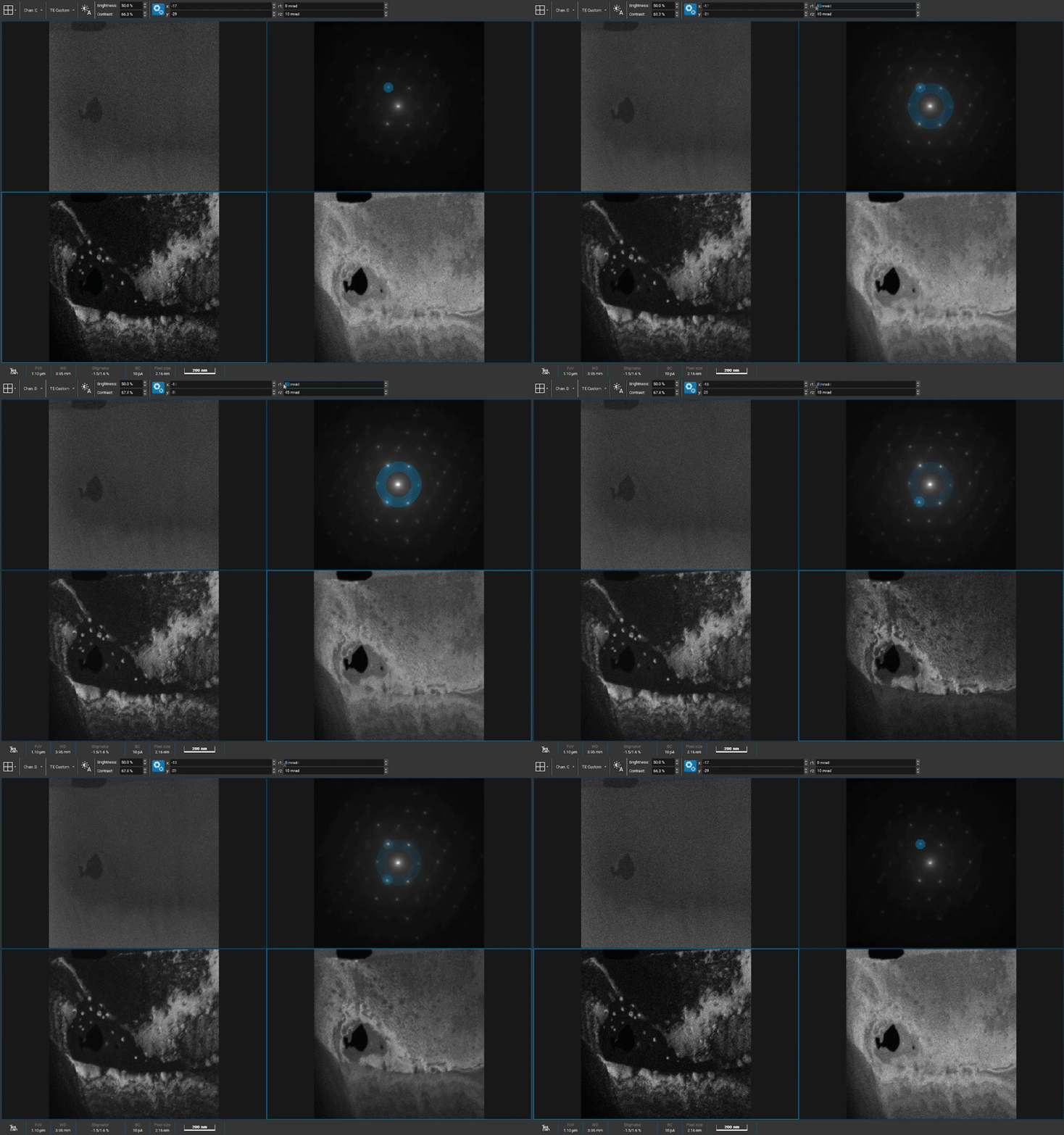
Virtual apertures enable live-view acquisition, allowing users to define custom bright-field and dark-field regions by selecting arbitrary angular ranges directly in Tescan Essence™ software for flexible, application-specific contrast optimization and extended imaging capabilities.

Seamless integration

Full hardware and software integration of the retractable 4D-STEM detector in AMBER™ 2 and AMBER X™ 2 platforms ensures intuitive, safe operation and seamless workflow control. The detector can be inserted or retracted with a single click in Tescan Essence™ software.

Unlocked content


Tescan Orage 2 APPLICATION EXAMPLES


[application examples in few words]


Unlock Tescan insight

leave a contact to access

Get the most out of Tescan

This is more than information; it's an advantage. We've compiled our technical whitepapers, detailed product flyers, and on-demand webinars to provide you with the knowledge that makes a real difference. Sign up now to access the insights you need to make an impact.

4D-STEM detector

Technical specification

Detector type

Solid state, hybrid pixel detector

Technology

Timepix 3 chip by AdvaScope, Peltier cooled

Chip parameters

256 × 256 pixel matrix; pixel size 55 µm × 55 µm

Detection limit

5 keV

Readout throughput

High throughput, 40 million hits·s¹·cm² 

Acquisition mode

 Data-driven 

Control

Fully integrated into Tescan EssenceTM, motorised

Image acquisition

Live imaging: up to 2 µs/pixel

2D imaging: Diffraction patterns and/or Kikuchi lines, Bright-Field and Dark-field imaging based on user-selectable virtual apertures

4D-STEM: data cubes

Protection

Integrated shutter and interlocks

Detector type

Solid state, hybrid pixel detector

Technology

Timepix 3 chip by AdvaScope, Peltier cooled

Chip parameters

256 × 256 pixel matrix; pixel size 55 µm × 55 µm

Detection limit

5 keV

Readout throughput

High throughput, 40 million hits·s¹·cm² 

Acquisition mode

 Data-driven 

Control

Fully integrated into Tescan EssenceTM, motorised

Image acquisition

Live imaging: up to 2 µs/pixel

2D imaging: Diffraction patterns and/or Kikuchi lines, Bright-Field and Dark-field imaging based on user-selectable virtual apertures

4D-STEM: data cubes

Protection

Integrated shutter and interlocks

4D_STEM_isolated_priruba_left_05-1024px

GET IN Touch

with specialist

map

Where you can find us:

Tescan Brno
Libušina třída 21
623 00 Brno
Czech Republic


130405923 us US 37.09024 -95.712891 25.3575 29.349345 20.67957527 42.082797 39.91384763 -33.693421 13.93320106 3.039986586 31.997988 38.050985 47.579533 48.1485965 58.375799 54.663142 19.195447 56.975106 47.916997 50.493053 45.868592 10.79556993 44.35660598 43.2371604 55.536415 14.557577179752773 32.100937 -6.116829 -6.212299277967318 33.600194 -12.08688 23.7104 -33.471062 31.998740087 -23.69149395 43.462349 51.529848 49.1893523 49.197486 25.072375 31.075811 1.299027 40.676979 52.30150662 51.013813 35.684121 37.566531 52.246622 40.581349 39.911632 -26.1811371 41.818215 33.429928

No distributors found.