
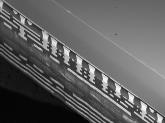
Advanced packaging failure analysis increasingly requires more than high-resolution imaging alone. As semiconductor packages integrate multiple dies, interfaces, interconnects, and materials in complex three-dimensional architectures, regions of interest can be buried deep within the device. Reaching them is only part of the challenge. Analysts also need to understand where those structures sit within the original device architecture and what has been exposed at each stage of sample preparation.
Explore Tescan workflows for semiconductor failure analysis and process control
The A15 workflow shown below connects nondestructive X-ray computed tomography (CT), ultrafast laser processing, optical and confocal microscopy, and scanning electron microscopy (SEM). Together, these techniques support progressive access to buried structures while preserving the spatial context needed to interpret them.
From CT Localization to Laser Access
The workflow begins with X-ray CT of an intact smartphone. The three-dimensional CT volume provides a navigation map for locating the A15 package, understanding its orientation and surrounding structures, and planning an access path before destructive preparation begins. It also provides a common spatial reference for subsequent preparation and microscopy stages.
Tescan FemtoChisel™ is then used to perform controlled laser decapsulation and overburden removal, exposing package-level features of DRAM circuitry and adjacent silicon structures.
Sequential laser delayering removes the upper DRAM circuitry, exposing the underlying silicon. Processing continues through the DRAM-associated silicon, revealing a second buried DRAM pair and ultimately reaching the interposer metallization. Multiple copper levels are then exposed step by step.
Image, Access, Verify, Decide
Microscopy guides the decisions between laser-processing steps.
Optical microscopy documents large-area geometry and exposed features. Confocal microscopy provides three-dimensional surface topography and depth information. SEM adds higher-resolution inspection of exposed circuitry, interfaces, and local structural details.
Together, these techniques support an iterative process:
Image → Access → Verify → Decide
Preserving Context for Semiconductor Failure Analysis
For advanced packaging failure analysis, reliability investigations, and security-oriented inspection, the value of an exposed feature increases when it can be related to its position within the original device. In the A15 workflow, CT establishes this spatial reference, while imaging at successive preparation stages helps analysts interpret the structures as they become accessible.
This continuity can help reduce uncertainty in target localization and sample preparation, supporting more informed decisions in failure analysis and reliability investigations. The workflow provides a way to reach deeply buried features while retaining the context needed to understand them.


Related Resources
Semiconductor Failure Analysis
Analyze buried semiconductor structures.

Tescan FemtoChisel™
Precision laser processing for sample preparation.