
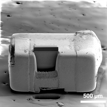
Multiscale imaging combines information from different length scales to understand a material's structure and properties. Researchers can move from millimeter-scale overviews to nanoscale details while preserving the relationship between features across the sample.
Listen to article
In the current opinion-rich media environment, providing contextual background to the data that underlies opinions is equally, if not more, important than providing the opinion itself. Therefore, it is critical that we focus not only on the data that are coming from the narrow field of interest but also on the broader context - the bigger picture so to speak - to avoid incorrect assumptions about a situation. This approach is especially valid in microscopy, which tempts scientists and engineers to focus only on the tiniest details in the materials they investigate, possibly resulting in incomplete conclusions.
But, suppose the cross section prepared by FIB is too small and made at a location without defects? Will our conclusion be that the material we produce is of flawless quality? And what if 3D tomography is performed on a small volume and at shallow depth, revealing small grains overall? Will we use this as a definitive confirmation of our hypotheses about the sample structure, even though the situation may ultimately vary across the entire width and depth of the area of interest?
Having information acquired from multiple scales and viewpoints provides you with the contextual information needed to form valid conclusions that result in better research outcomes or optimized future products. We demonstrate this premise in Figure 1, which shows two images of the same polished cross section. Looking at these images independently, we might conclude from sample 1a that the surface contains minimal defects. In contrast, Figure 1b shows a greater number of defects.
Viewing this same cross section at a lower magnification clearly demonstrates the necessity of a multiscale approach when analyzing defects in materials. If only the smaller cross section area is investigated, we may wrongly assume that the overall quality of the MLCC microelectronic device is good. A larger field of view will reveal the true presence of defects in the sample and their distribution, which leads to a completely different conclusion about the quality of the material.
In the multiscale approach, you can use Scanning Electron Microscopy (SEM) to investigate features well below <50 nm, recording their size, topography, material contrast, or composition. You can also document their location on the sample (often in a mm-size area), their overall distribution, and heterogeneity across the sample surface. This applies equally to Focused Ion Beam–Scanning Electron Microscopes (FIB-SEM) where, in addition to surface characterization, the multiscale approach can be applied to sub-surface applications such as cross-sectioning or 3D FIB-SEM tomography.
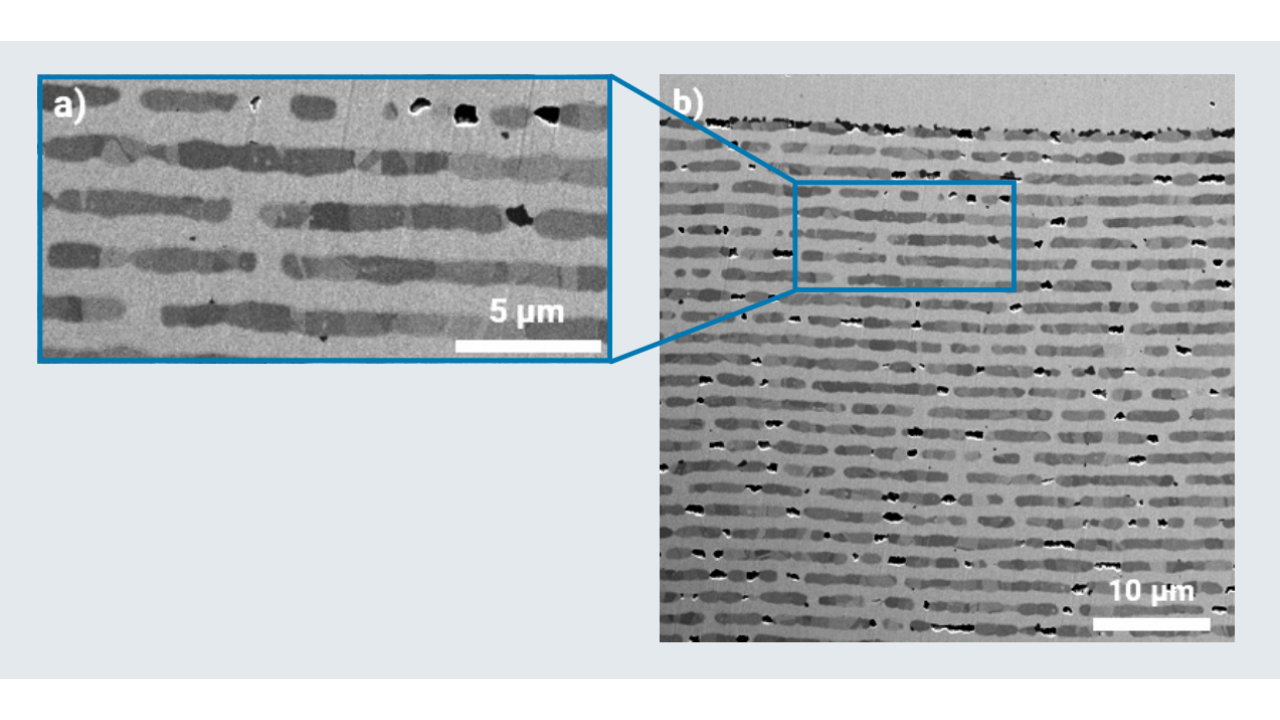 Figure 1: FIB-SEM cut through the layers of an MLCC electronic device.
a) This high magnification view of a 10 × 20 µm area from the polished cross section appears to show a surface with minimal defects in the material. b) By viewing at a lower magnification, we now see numerous defects and their distribution.
New to FIB-SEM? Learn how FIB-SEM combines electron imaging and ion beam milling for advanced materials characterization.
How Does Multiscale Imaging Improve Surface Contrast?
Electron microscopy is used primarily to explore samples at the nanoscale, enabling characterization of the tiniest details at high magnification. This often helps in understanding material structure and its implications for the physical and mechanical properties or overall quality of the materials.
Nevertheless, acquiring data with only a narrow field of view and at high magnification may lead to misleading conclusions. It is also the contextual information, obtained at the macro-scale, that helps us determine the complete picture. The wider field of view gives us information about the location of the specific feature on which we are focused and provides us with more reliable statistical information about the material.
In Figure 2, you can see how different levels of magnification revealed crucial information about the tungsten carbide magnetic powder sample. The image at the highest magnification (Figure 2a) provides a detailed view of the sample surface and reveals small particles of a few nanometers in size. Looking at the sample from a wider field of view (Figure 2b), it is clear that the particles differ significantly in their sizes and shapes, and that they are non-uniformly distributed.
By zooming out to a micron-scale view (Figure 2c), it is evident that nanoparticles are part of a large, globular cluster. Considering that these particles are used as a precursor material, we need all of the aforementioned data to predict the final material characteristics and adjust our production process accordingly.
This is a clear example of how important it is to acquire data at multiple scales. Acquisition of a single image at high magnification could lead to incomplete characterization of the specimen, which may result in incorrect conclusions.
At the same time, these characterizations are made using various contrast methods. Therefore, the ability to differentiate contrast based on angle and energy provides additional information. Extending acquisition to include dedicated analytical detectors brings a new level of understanding and adds the multimodality that is frequently leveraged for the evaluation of materials.
Each of these contrast and analytical methods contributes to this multiscale approach and is made possible using an SEM column with ultra-high resolution (UHR) capability.
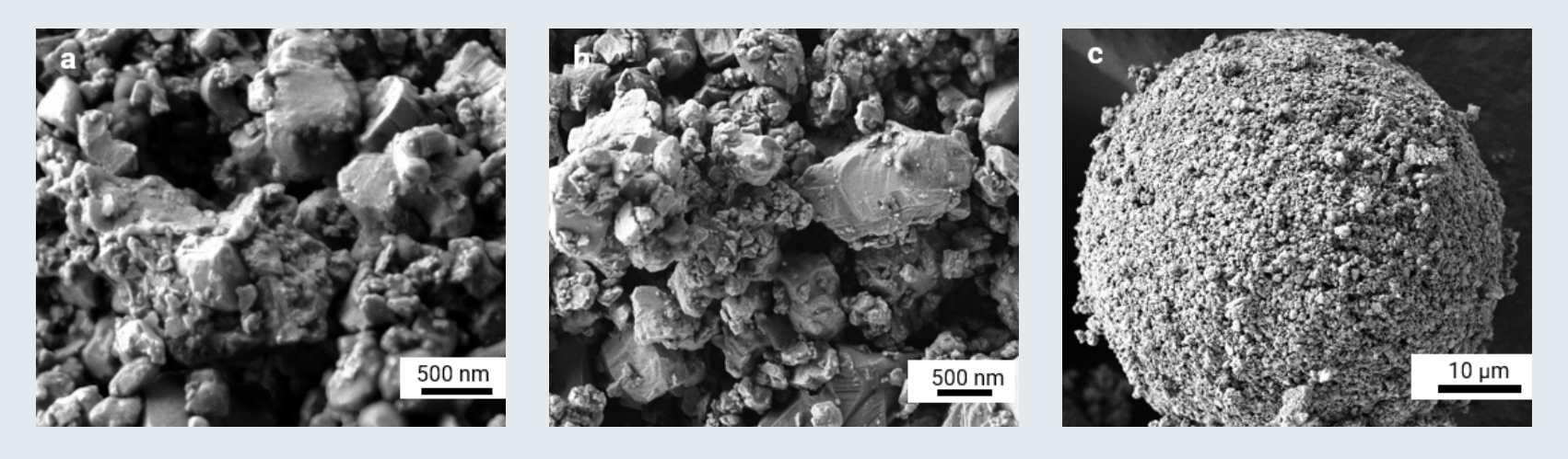 Figure 2: SEM image of a magnetic tungsten carbide sample acquired at different magnifications, imaged at 2 keV accelerating voltage.
Learn more: Explore why automated TEM lamella preparation with FIB-SEM is only part of the workflow, and how final specimen quality affects reliable S/TEM analysis.
How FIB-SEM Extends Materials Characterization from 2D to 3D
FIB-SEM is designed to perform site-specific cross-sectioning, sample fabrication, and sample modification with an ion beam, either gallium FIB or Xe plasma FIB. This extends characterization to below the sample surface. Using FIB to precisely remove material permits access to the sample’s Z dimension, which leads to more comprehensive data from the sample.
Usually, these data can be obtained from a single cross section, 3D FIB-SEM tomography reconstructions, prefabricated micro-testing specimens, or from TEM/STEM samples.
Cross-sectional and 3D tomography data often contain both detailed and multiscale information. Therefore, to understand a feature or other details in context, it is important that the target area is representative of the studied feature. It must contain enough statistical data to be relevant for determining overall material characteristics.
In general, the parameters of a cross section or 3D tomography are defined based on the features of interest in the sample. These parameters vary from sample to sample. For instance, in the case of metal samples containing conventional-sized grains around several micrometers to tens of micrometers, the volume required for investigation may be as large as 500 × 500 × 500 µm³.
Smaller grains, such as those in the sub-micrometer size range, require a smaller analyzed volume. Nevertheless, a larger area still provides benefits through improved statistics and a clearer understanding of the material’s crystallography or phase distribution.
In addition, features of interest may occur deep within the sample, and a wide cross section without sufficient depth will not provide the relevant information.
How to Characterize Features Deep Inside a Material
A large-sized feature of interest, or a feature located deep within a material, almost always dictates the necessity for a large and deep cross section. An example of such materials science samples are structured materials or composites that contain multiple layers or a thick coating.
Samples like this require the removal of large volumes of material to access and visualize localized defects and other details within the context of the surrounding material. The example in Figure 3 demonstrates this approach.
MLCC microelectronic components consist of multiple metallic and ceramic layers with a total thickness of 300 µm. This layered system is embedded deep within the structure. A large area was removed to create a cross section of sufficient size to visualize the stack of layers and search for defects in the structure.
In this case, a cross section 500 µm wide and more than 300 µm deep was prepared, as shown in the image. Despite the possibility of analyzing detailed information deeper within the material, it is evident that a large area had to be uncovered first to obtain enough statistical data about the sample and reveal the defect distribution over a larger area.
This same process is required for coatings, multilayer materials, and many alloys. For these materials and similar applications, it is essential to capture all characteristics and interfaces within a statistically representative volume to evaluate defects and adhesion.
This necessitates a multiscale approach, as both the location and distribution of features in relation to the surrounding material provide critical data for making accurate conclusions.
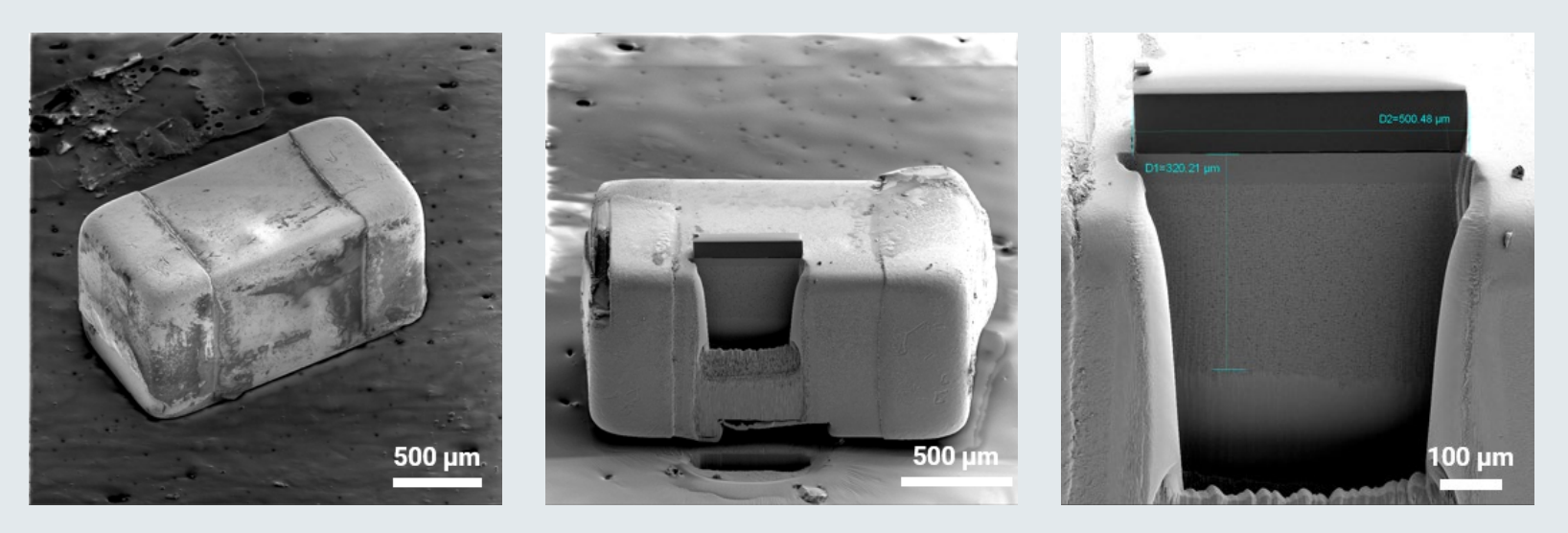 Figure 3: MLCC electronic component analyzed through the metal/ceramic layers embedded within the device.
How Large-Volume 3D FIB-SEM Reveals Hidden Material Features
A statistically meaningful representation of the results is an essential parameter for qualified decision-making in materials science. This is also true for FIB-SEM analysis of materials, where, as mentioned previously, the structure and features determine how large the analyzed volume must be for materials evaluation.
The area for analysis can be determined based on several parameters. When the area of interest is a repetitive structure within the sample, the minimum analyzed volume can be established based on the number of features required to ensure accurate representation of all structures in the sample.
This is not a significant challenge for nanoscale features, as a volume of several µm³ may be sufficient. However, for microscale features, a small volume may not be representative of the entire sample being analyzed. Small volumes instead provide valuable data mainly for homogeneous samples containing small features.
The situation is completely different when features vary across a large sample surface or when large features of interest need to be analyzed.
Figure 4 shows the analysis of the shell structure of Argonauta hians. The shell structure was characterized using contrast around the grain boundaries. The grain size distribution varied substantially across the sample volume, but the expected average grain size was approximately 500 nm in diameter.
To validate the grain size, material contrast was used to identify the nanometer-thick grain boundaries. To achieve a high level of detail within a large volume, analyses were performed using a larger field of view (Figure 4).
3D FIB-SEM tomography provides more data for analysis, leading in this case to accurate scientific conclusions about the grain sizes. Furthermore, analyzing the large volume revealed additional parameters that were not previously known: the dominant orientation of the grains.
This information would not have been possible to obtain from analysis of a small volume. Determining grain orientation in both space and shape provided a deeper understanding of the material characteristics and the grain growth process.
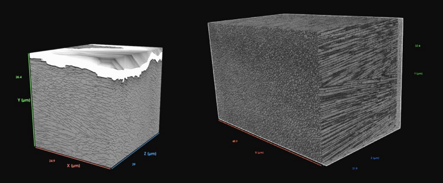 Figure 4: 3D FIB-SEM tomography reconstruction of the Argonauta hians shell sample. a) Smaller reconstructed volume: 26 × 25 × 29 µm³. b) Larger reconstructed volume: 49 × 32 × 32 µm³. (The Argonauta hians specimen is courtesy of Prof. Antonio Checa, University of Granada, Spain.)
Learn more: See how researchers at CEITEC Nano combine FIB-SEM and SIMS to support multimodal characterization across advanced research workflows.
How to Achieve Representative 3D Materials Analysis
Materials are designed to match the mechanical or physical properties required for their intended function. In the case of cutting tools, the coating material is designed to be durable so that it can cut through hard materials without damaging the sharp edge of the tool. The same cutting tool may also require greater material toughness in the central part of the tool.
Therefore, we can assume that material chemistry, grain size distribution, and material phases are adjusted according to their position within the tool. Studying larger areas of the sample helps us understand changes in properties that are relevant to the functionality of the entire tool, device, or component.
The analysis of larger areas becomes especially important when material properties change gradually. Such gradual changes may occur during material preparation as a result of chemical or heat treatment, or through the application of external forces during material formation. Analyzing a larger area provides more precise information than extrapolating results from smaller measurements.
The example in Figure 5 shows 3D EBSD analysis of cold-drawn copper wire. EBSD analysis allows us to precisely define phase distribution within the material, similar to how grain size distribution is determined. 3D FIB-SEM tomography provides the dimensional context that is missing from 2D data, which is essential for studying and understanding grain shape and orientation within the material.
By analyzing the complete volume, we can accurately evaluate data related to the position of features within the sample. For this sample, if only small datasets were prepared, we would obtain information relevant only to the outer region of the wire, a few micrometers below the surface.
To visualize and analyze the inner structure, the wire can be sectioned using FIB.3D EBSD FIB-SEM tomography allows reconstruction of not only the entire volume but also individual grains within the material.
This analysis reveals not only variations in grain size distribution but also the presence of two different grain shapes. With this contextual information, we can predict the material’s mechanical properties and extrapolate the findings to the entire volume.
The relative positions and distribution of different grain sizes allow us to predict material properties across the whole sample from a statistical perspective. In this example of cold-drawn copper wire, we can validate that the material preparation process resulted in the grain size and grain shape distribution revealed by the 3D EBSD data.
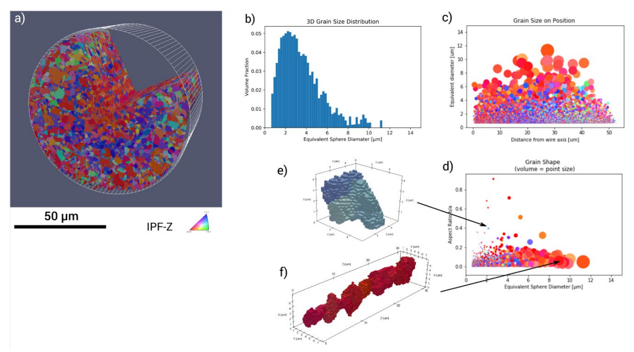 Figure 5: 3D EBSD FIB-SEM tomography analysis of cold-drawn wire.
a) 3D EBSD FIB-SEM tomography of cold-drawn wire. b) 3D grain size distribution. c) Grain size based on position. d) Grain shape analysis. e–f) 3D grain reconstruction.
How Electron Microscopy Enables Multiscale Materials Characterization
Collecting data from multiple scales, with adequate contextual information, is essential for forming valid conclusions that lead to better research outcomes or optimized future products. Using SEM to understand feature size, topography, material contrast, or composition is important. However, it is equally important to understand a feature’s location within the sample, as well as its overall distribution and heterogeneity across the sample surface, to make reliable conclusions about the material being evaluated.
With FIB-SEM, the multiscale approach can also be applied to subsurface applications such as cross-sectioning and 3D FIB-SEM tomography.
Some fields of application, such as research on metals, ceramics, hard coatings, and other materials science studies, require advanced analytical characterization capabilities. Other fields, such as semiconductor research, require the highest possible resolution for imaging and failure analysis.
In theory, improvements focused on one application area might limit performance in others. However, Tescan FIB-SEM instruments are designed to address this multiscale and multimodal challenge in materials science while maintaining maximum flexibility and superior SEM resolution.
Tescan’s unique Ultra High Resolution BrightBeam™ column, featured on Tescan AMBER FIB-SEM and Tescan AMBER X plasma FIB-SEM systems, enables observation of a wide range of samples, including magnetic materials, while supporting multiscale characterization through the Wide Field Optics™ design.
This extends superior UHR imaging capabilities to large field-of-view imaging and improves analytical techniques by maintaining high resolution while using high analytical currents. Wide Field Optics is especially valuable for navigation and large-area analyses.
The Tescan BrightBeam™ SEM column is equipped with a comprehensive set of in-column and chamber electron detectors capable of acquiring up to eight signals simultaneously, providing valuable sample contrast information. As an analytical column, it is designed to reach currents of up to 400 nA, accelerating the acquisition of EDS and EBSD data.
On the FIB side, both Ga FIB-SEM and Xe plasma FIB-SEM systems support multiscale investigations. Ga FIB-SEM systems can reach maximum currents of around 100 nA, making them suitable for material removal and preparation of cross sections in the range of tens of micrometers.
When larger cross sections are required, Xe plasma FIB can be considered, as it can reach up to 3 µA maximum FIB current and prepare large areas in the range of hundreds of micrometers.
Tescan FIB-SEM instruments also support multimodal analysis techniques such as EDX, EBSD, ToF-SIMS, and RAMAN, extending the range of analytical information that can be collected during multiscale investigations.
Conclusion
With these capabilities for obtaining multiscale and multimodal information about your materials, you can improve processes and enhance research by gaining detailed insights into features within the context of their presence across a larger area or the entire material sample.
This deeper characterization of materials and their properties allows us to better understand the physical and chemical processes occurring during material creation and throughout real-world use.
This knowledge can be applied not only to the design of new materials but also to the development of tools, components, and devices that perform exactly as intended.


Related Resources
FIB-SEM Portfolio
Explore FIB-SEM solutions for advanced materials characterization

Advancing TEM Sample Preparation
Learn how AMBER™ 2 improves TEM specimen preparation.

Ar⁺ Polishing for TEM Preparation
Improve TEM specimen quality with gentle Ar⁺ polishing.

APT Specimen Preparation
Prepare site-specific APT specimens with AMBER™ X 2.