Abstract
Ga⁺ FIB-SEM has made site-specific TEM lamella preparation precise, flexible, and highly effective. It allows users to prepare thin specimens from the exact region of interest with nanometer-scale control. But the same gallium ions that make this possible also limit what can be achieved at the same time. During FIB milling, Ga⁺ amorphize the specimen surface, become implanted in the material, and modify the region that later needs to be analysed in S/TEM.
That represents the Ga⁺ ceiling in TEM lamella preparation. Even when the lamella is thin enough, its surface may still contain FIB preparation-induced damage that can affect high-resolution imaging, EDS, or EELS analysis. Tescan AURA™ Gentle Ion Beam addresses this final limitation by introducing low-energy Ar⁺ cleaning directly into the FIB-SEM workflow. It does not replace Ga⁺ preparation process. It completes it by providing a gentle, gradual, and highly controllable way to remove the Ga⁺ induced damaged surface layer step by step. With low-energy, chemically inert Ar⁺ polishing, the lamella can be finished layer by layer without introducing the same type of additional damage associated with Ga⁺ milling. The result is a lamella that is not only ultra-thin, but also cleaner and reliable for real high-resolution S/TEM analysis.
Introduction
Ga⁺ FIB-SEM has become one of the most important methods for site-specific S/TEM specimen preparation because of its precision, flexibility, and speed. It allows users to extract a lamella from the exact region of interest and thin it down to electron transparency with nanometer-scale control.
But Ga⁺ FIB-SEM milling has a natural limit. The same gallium ions that make precise milling possible also interact with the sample and can modify the very surface that must later be analysed in S/TEM.
This is not mainly a problem of poor workflow or insufficient automation. It is a consequence of ion-solid interactions.
When Ga⁺ ions strike a specimen, they transfer energy into the material, displace atoms, become implanted, and can create an amorphous or chemically modified surface layer. For many S/TEM applications, this altered layer is exactly where the most important information should be coming from.
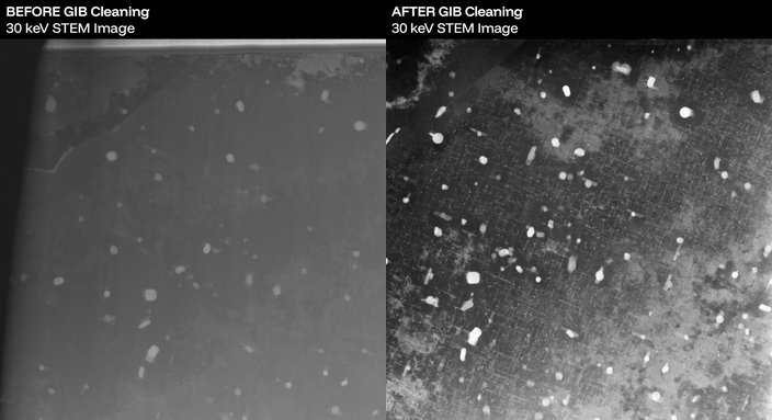
Learn how automated TEM lamella preparation with FIB-SEM can be combined with final specimen cleaning to improve consistency and TEM analysis quality.
What is Behind Ga⁺ FIB Sample Damage?
The need for gentle ion beam cleaning starts with a simple physical fact: an ion beam does not only remove material. It also changes the material surface.
When an ion hits a solid, its kinetic energy is transferred to the atoms in the specimen. This energy spreads through a small volume called the collision cascade. Inside this cascade, atoms can be displaced from their lattice positions, defects can be generated, and part of the incoming ion species can remain implanted in the material.
The depth and severity of this damage depend mainly on the ion energy, ion mass, beam geometry, and target material. High-energy ions penetrate deeper and create thicker damaged layers. Lower-energy ions affect only the near-surface region.
For Ga⁺ FIB-SEM specimen preparation, this matters because gallium is not just a physical milling species. It is also a reactive element. Implanted Ga⁺ can alter local chemistry, segregate to grain boundaries and interfaces, and in sensitive materials such as aluminium alloys, compound semiconductors, or multi-phase systems, it can change the microstructure that the user wants to study. Figure 1 illustrates this process by showing how sputtering, Ga implantation, atomic displacement, and the collision cascade occur beneath the milled surface.
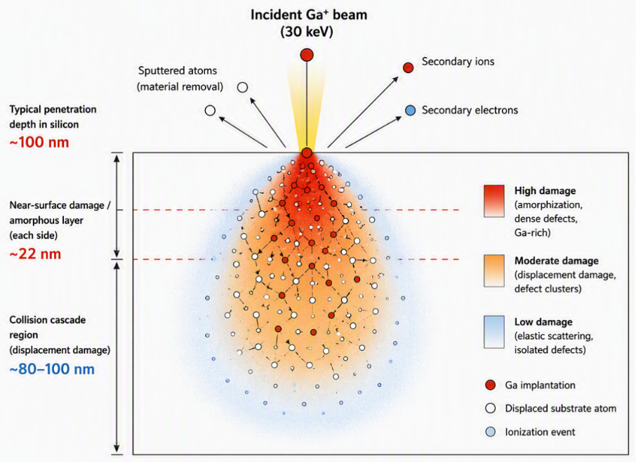 Figure 1. What 30 keV Ga⁺ milling does to silicon. Schematic representation of ion-solid interactions during Ga⁺ FIB milling, showing surface sputtering, secondary-ion and secondary-electron emission, Ga⁺ implantation, atom displacement, and the resulting collision cascade beneath the specimen surface. The illustration distinguishes the near-surface amorphous and Ga-rich damage layer from the deeper region affected by displacement events and isolated defects. Dimensions are indicative and depend on material and milling conditions. Illustrative model (AI-generated). Damage zones and depths reflect standard literature values for Si, not direct simulation.
This is why Ga⁺ damage is not only an imaging artifact. It can become an interpretation problem. The analysed signal may include information from a surface layer that was partly created by the preparation process itself.
In other words, the specimen may be thin enough for S/TEM, but not clean enough to fully represent the original material.
From Ga⁺ Damage to Low-keV Ar⁺ Cleaning: Why the Finest TEM Lamella Needs a Different Ion
In practice, FIB-SEM works extremely well for sample fabrication such as TEM lamellae. Ga⁺ ions are commonly accelerated at 30 keV for high-resolution, site-specific milling. This is exactly what makes Ga⁺ FIB-SEM so useful: the beam can cut, shape, and thin a lamella with nanometer-scale precision. However, this same energy also drives ions deeper into the specimen sidewalls and creates a damaged surface region.
For silicon, published data show that 30 keV Ga⁺ milling can produce an amorphous layer approximately 22 nm thick on each side of the lamella. That number becomes critical in applications where high-quality STEM imaging requires the total specimen thickness to remain below about 50 nm.
The problem is easy to understand. If each side of a thin specimen contains around 22 nm of damaged material, then most of the lamella may no longer represent the undisturbed structure. The microscope can still produce an image, but the specimen itself has been heavily modified before analysis.
This is especially problematic for atomic-resolution imaging, EDS, EELS, layer interfaces, thin films, grain boundaries, and small semiconductor structures, where the region of interest may be only a few nanometers wide.
The obvious solution is to reduce the Ga⁺ energy during the final cleaning steps. This helps: 5 keV or 2 keV Ga⁺ polishing creates a thinner damaged layer than 30 keV milling, but it does not remove the fundamental limitation - gallium is still the final ion species interacting with the sample. Some amorphization, implantation, or chemistry-related modification remain.
This is the Ga⁺ ceiling: Even with careful low-keV Ga⁺ finishing, the final quality is still limited by the interaction between gallium ions and the specimen.
This is where low-keV Ar⁺ cleaning becomes necessary. Argon is not used because it replaces the value of Ga⁺ FIB-SEM. Ga⁺ remains the right tool for precise, site-specific lamella preparation. Ar⁺ is used because it is better suited for the last few nanometers of surface refinement, where the goal is no longer shaping the specimen, but removing preparation-induced damage as gently as possible.
Low-energy Ar⁺ polishing offers two key advantages at this stage. First, the interaction is shallow. At energies below about 500 eV, the collision cascade is confined to the near-surface region as thin as 1 nm, so Ar⁺ can remove the Ga-damaged outer layer without creating a new deep damage zone. Second, argon is chemically inert. It does not alloy with the specimen, does not form Ga-rich interfaces, and does not introduce a reactive species into the region that will later be analysed.
For materials such as aluminium alloys, copper, germanium, Ga-containing semiconductors, thin films, multilayers, and interfaces, this matters directly. These are cases where the difference between a damaged surface and a clean crystalline surface can determine whether the final S/TEM result is trustworthy.
Low-energy Ar⁺ polishing therefore works as a damage-replacement step. It removes the thicker Ga-damaged layer and replaces it with a much thinner, inert-ion polishing effect. The goal is not to claim that any ion beam is completely damage-free. The goal is to push the remaining disturbed layer below the level that would affect atomic-resolution imaging and analysis.
This is why the term “gentle” is important. Gentle does not simply mean slow or weak. It means that the final ion interaction is shallow, chemically inert, and controlled enough to clean the surface without reintroducing the same type of artefacts that the process is trying to remove. Figure 2 shows how much of a thin 50 nm lamella can remain affected by damaged sidewall layers after different ion-processing steps.
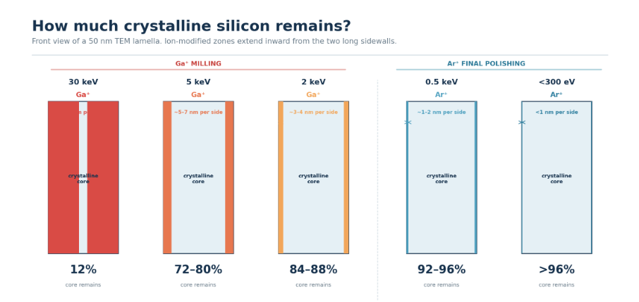 Figure 2. Schematic comparison of the fraction of a 50 nm silicon TEM lamella that remains crystalline after preparation with Ga⁺ and Ar⁺ ions. Damage layers are shown proportionally on the left and right sidewalls. Lower-energy Ar⁺ processing preserves significantly more of the original specimen than conventional Ga⁺ milling. This schematic is an AI-generated visualization of a theoretical 50 nm lamella, using established literature values to calculate the remaining crystalline proportions.
Learn more about why integrating Ar⁺ cleaning with Ga⁺ FIB-SEM can improve the final quality of advanced S/TEM specimens.
From Ga⁺ Milling to Ar⁺ Cleaning: What Aura™ Adds
Aura™ Gentle Ion Beam builds on this physical advantage by integrating low-energy broad-beam Ar⁺ polishing directly inside the FIB-SEM workflow (Figure 3). This is important because the final TEM lamella is most fragile exactly when it needs cleaning. If the user must move it to a separate polishing tool, the workflow gains risk: sample transfer, contamination, misalignment, additional setup, and possible specimen loss.
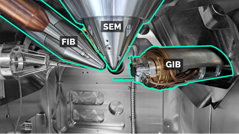 Figure 3. FIB-SEM chamber interior showing the FIB, SEM columns and Aura™ Gentle Ion Beam (GIB) focusing to the same coincidence point. This integration enables in-chamber Ar⁺ gentle ion beam cleaning directly after Ga⁺ FIB-SEM lamella preparation, without transferring the specimen to a separate polishing tool.
With Aura™, the user can keep the lamella inside the same system, move from Ga⁺ preparation to Ar⁺ final cleaning, and verify the result in one connected workflow. Aura™ combines low-energy argon polishing, integrated positioning, recipe-based operation, and in-system quality control to reduce workflow fragmentation and improve the chance of achieving the required specimen quality the first time.
That creates three practical benefits: (1) Aura™ helps reduce Ga-induced artifacts by removing the damaged surface layer with inert Ar⁺. (2) It improves usability because final polishing becomes less dependent on difficult low-keV Ga⁺ imaging, polishing-window placement, and expert judgement. (3) It improves repeatability because the final cleaning step can be performed as part of a controlled, recipe-based workflow rather than as a separate manual process.
This is the key: Aura™ does not replace Ga⁺ FIB-SEM. It completes it. Ga⁺ remains the tool for precise, site-specific lamella preparation. Aura™ adds the lower-damage final cleaning step that helps preserve the specimen surface for the analysis that follows.
Written by Petr Klimek, PhD
Product Marketing Director, Tescan


Related Resources
AURA™ Gentle Ion Beam
Low-energy argon polishing for high-quality TEM specimens.

Ultra-Thin TEM Lamella Preparation
See integrated FIB-SEM and argon polishing in action.

Ar⁺ Polishing for TEM Sample Preparation
See how Ar⁺ polishing improves TEM specimen quality.

FIB-SEM Systems
Explore solutions for precision imaging and sample preparation.