
Enhancing Ga+ FIB-SEM Capabilities with Fully Integrated Low-Energy Argon Ion Beam Cleaning
Introduction
The progression of modern materials science is increasingly defined by the ability to characterize structures at the nanometer and atomic scale levels. As the complexity of multi-phase alloys, ceramic and other heterostructures increases and physical dimensions of semiconductor devices shrink into the sub-5 nanometer regime, the demand for pristine specimen preparation for scanning/transmission electron microscopy (S/TEM) has become essential. For decades, the primary constraints in S/TEM have not necessarily been the imaging resolution or analytical capabilities, but rather the "specimen transparency bottleneck"- the challenge of producing a specimen that is thin enough while remaining representative of the bulk material’s intrinsic structure. If features as small as 10 nm are required in the final specimen thickness, then dependable, repeatable methods for producing <50 nm-thick specimens with minimal damage are essential for modern S/TEM specimen preparation.
Currently, the Focused Ion Beam (FIB) is a go-to solution for high throughput, automated, site-specific specimen preparation, allowing researchers to extract lamellae from any area of interest with nanometer-scale accuracy. However, for FIB-SEMs with a Ga+ ion source, Ga+ ions may introduce surface amorphization, ion implantation, and chemical segregation, which can obscure atomic resolution and may even compromise analytical spectroscopic data such as Energy Dispersive X-ray Spectrometry (EDS) and Electron Energy Loss Spectroscopy (EELS). To address these limitations, low-energy Ar+ ion-beam polishing can be used to mitigate the challenges posed by Ga+ ion milling alone. By utilizing inert gas Ar+ ions at accelerating energies below those typically available in a Ga+ ion FIB (typically in the range 100 to 500 eV), Ga-implanted surface layers can be gradually removed, achieving ultra-thin, low-damage specimens from any material required for (S)TEM imaging and analysis.
Challenges related to Ga+ FIB SEM milling
The Physics of Ion-Solid Interactions
The necessity of gentle ion beam cleaning arises from the deterministic physics of ion-solid interactions. When an ion impacts a target material, its kinetic energy is dissipated through a series of elastic and inelastic collisions with the target atoms, within a region defined by this collision cascade. The depth of this collision cascade and the resulting displacement of recoil lattice atoms are direct functions of the incident ion's energy and mass and will determine the type and depth of damage to the target. Ion implantation is an unavoidable consequence of any species of ion milling, and in some materials, a metastable amorphous layer can form as a result of the ion bombardment. Since Ga is a reactive species, its implantation can alter surface properties. As an example, Ga demonstrates a pronounced affinity for segregation to grain boundaries and interphase interfaces, particularly in Al-alloys, which can change the local microstructure and impact material performance.
The practical process of preparing samples with Ga+ FIB illustrates these theoretical concepts, highlighting both advantages and disadvantages. In FIB-SEM S/TEM specimen preparation, Ga+ ions are typically accelerated at 30 keV to achieve the highest resolution beam. This energy enables precise nanometer-scale milling but also causes enough momentum to displace atoms deep in the lattice, forming a metastable amorphous layer along the specimen sidewalls. On silicon substrates, a 30 keV Ga+ beam produces an amorphous layer of ~22 nm thickness on each side. Since high-quality STEM imaging often requires a total specimen thickness below 50 nm, the presence of a 22 nm damage layer on both surfaces renders the specimen almost entirely amorphous, effectively compromising the region of interest. Therefore, low keV cleaning procedures are applied; whereby thick high energy ion damage layers are milled and replaced by sequentially lower energy ions to reduce the sidewall damage with each reduction in beam energy.
The Necessity for Low-keV Ar Processing
The transition to low-keV Ar+ ion processing was motivated by the fact that lower energy Ar+ ions are available compared to Ga+ ions and Ar is inert. Therefore, as the Ar+ ion energy is reduced < 500 eV, the ion collision cascade is confined to the immediate few nanometers of the specimen surface. Research has demonstrated that reducing the ion energy <300 eV can yield amorphous layers thinner than 1 nm which is even below what is achievable by the low energies typically available via Ga+ FIB low keV Cleaning and is well within the tolerance for any atomic-resolution imaging and analysis requirements.
In addition, as an inert gas, Ar+ does not form chemical bonds with any substrate, avoiding the alloying artifacts associated with Ga+. So, the use of Ar+ ions for final polishing effectively replaces any Ga+ enriched surface layer previously leaving behind a low-damage crystalline surface for analysis.
| Ion Energy (keV) | Ion Species | Damage Layer Thickness (nm) | Modification of material by Ions |
|
30 keV |
Ga+ |
22 nm |
amorphization |
|
5 keV |
Ga+ |
5 – 7 nm |
amorphization |
|
2 keV |
Ga+ |
3 - 4 nm |
amorphization |
|
0.5 keV |
Ar+ |
1 – 2 nm |
Negligible |
|
<300 keV |
Ar+ |
< 1 nm |
Negligible |
Table 1: Summary of measured damage layers, compiled from published sources, measured for Silicon specimen1;2.
Performance Across Different Material Systems
The use of Ar+ ions for low keV cleaning proves highly effective and beneficial for various materials and applications.
Metals and Alloys: Managing Point Defects and Ga induced damage
Metals typically retain their crystalline structure even when exposed to high-energy Ga+ FIB-SEM bombardment. Consequently, the formation and thickness of an amorphous layer is not the primary concern; rather, metals tend to develop dense networks of point defects due to the ion bombardment and recoil motion within the collision cascade. For example, Al-Cu alloys, Aluminum Oxide, and stainless steels exhibit reactions between aluminum and Ga+ implantation. To address Ga+ contamination, Ar+ milling at low acceleration energies (<500 eV) is employed to effectively clean the surface and reduce crystalline imperfections. This process removes the Ga produced defect layer and uncovers sub-nanometer precipitates and other critical features that would otherwise remain concealed (see Figure 1 and Figure 2).
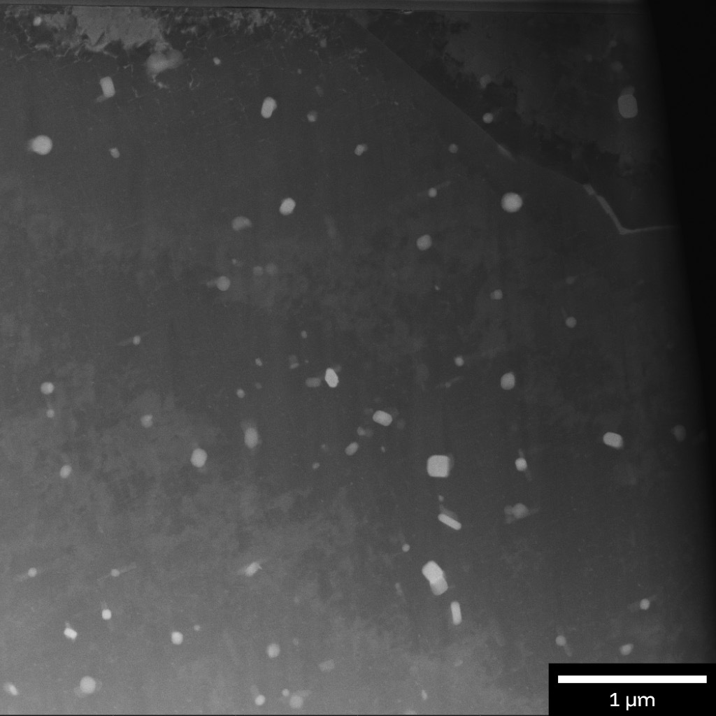
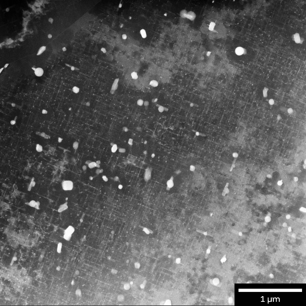
Figure 1. Al Alloy specimen prepared by low keV Ga+ FIB milling (left) and Gentle Ion beam cleaning (right) (Image courtesy from Ben Britton, University of British Columbia)
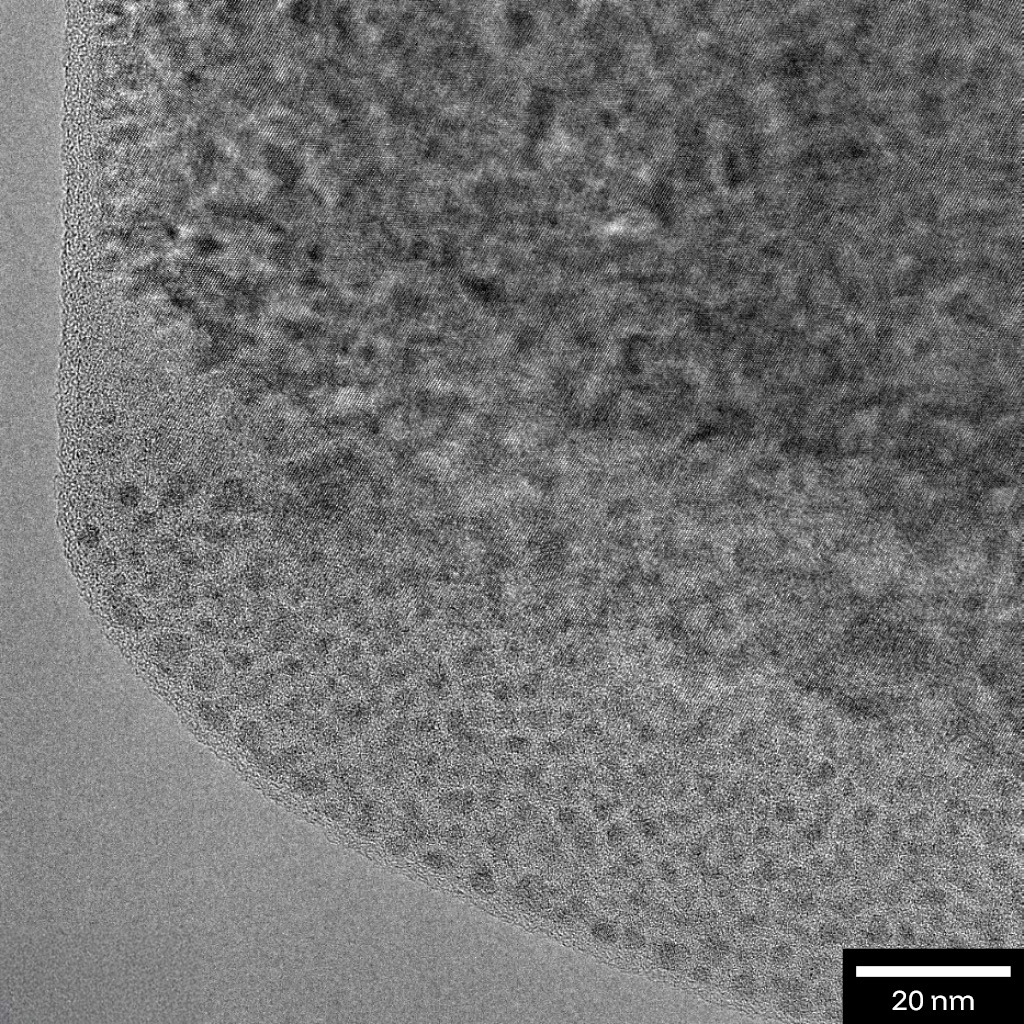
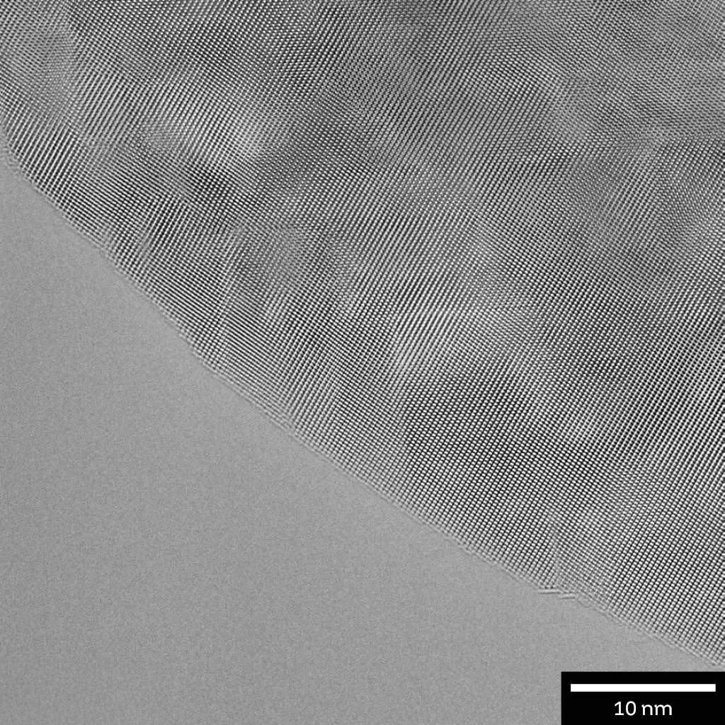
Figure 2. Al2O3 TEM Specimen without (left) and with Ar Broad Ion Beam Polishing (right). (Image from Technoorg Linda)
Semiconductors: Silicon, Germanium, Gallium
Semiconductors are cleaned with Ar+ ions because they are highly prone to amorphization and react easily due to their chemical nature and layered composition. For composite device characterization - such as studying the interface between a silicon (Si) substrate and a germanium (Ge) heterostructure - using higher-energy Ga+ focused ion beam (FIB) techniques can obscure the crucial atomic layers at the interface.
Low-energy Ar+ polishing at 500 eV is an effective method for thinning samples to less than 20 nm while preserving lattice structure across interfaces. For materials like germanium (Ge), Aluminum Nitride, and gallium nitride (GaN), which are more vulnerable to displacement damage than Silicon, even lower energies - often below 500 eV - are necessary to avoid forming Ga-rich metallic droplets or causing surface roughness (see Figure 3).
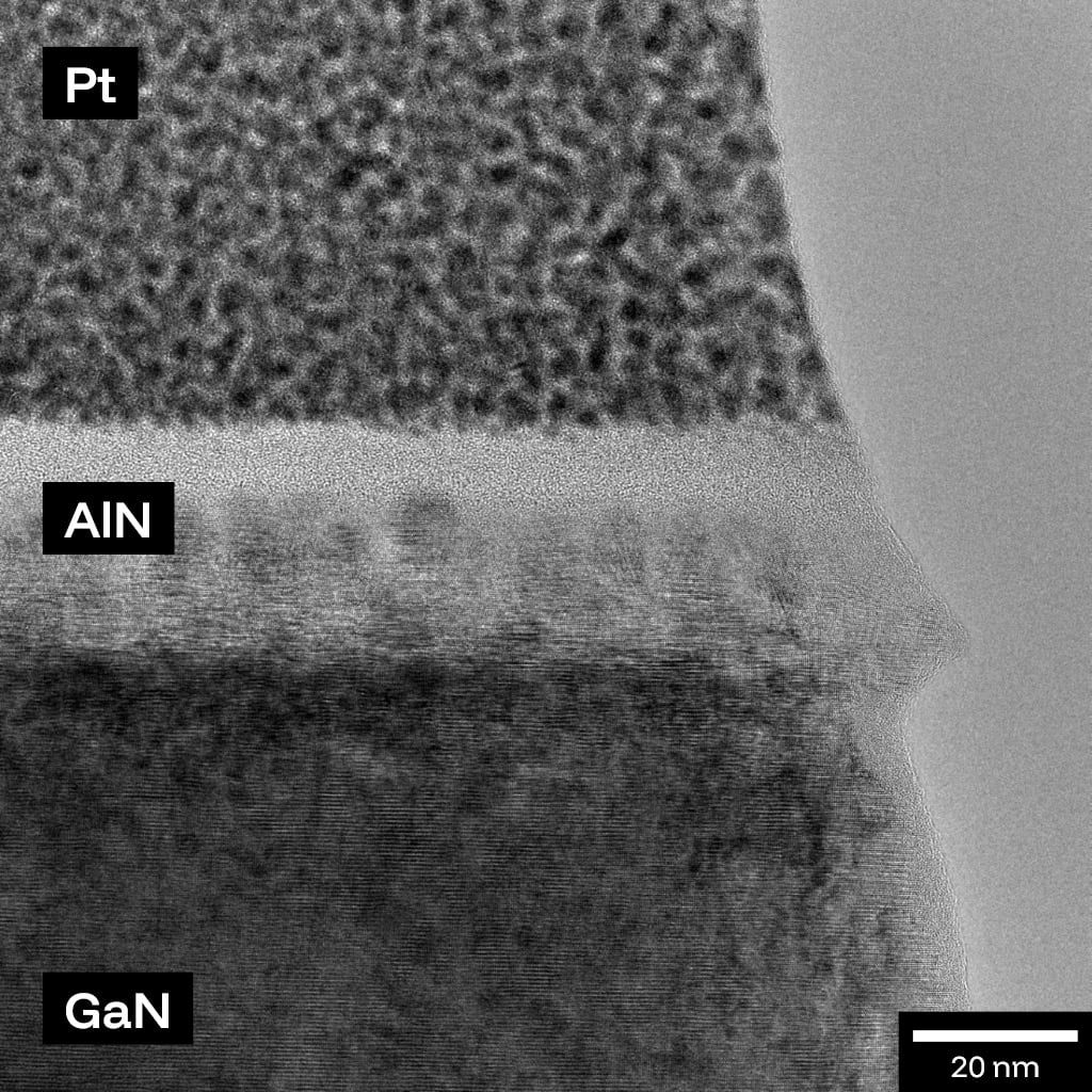
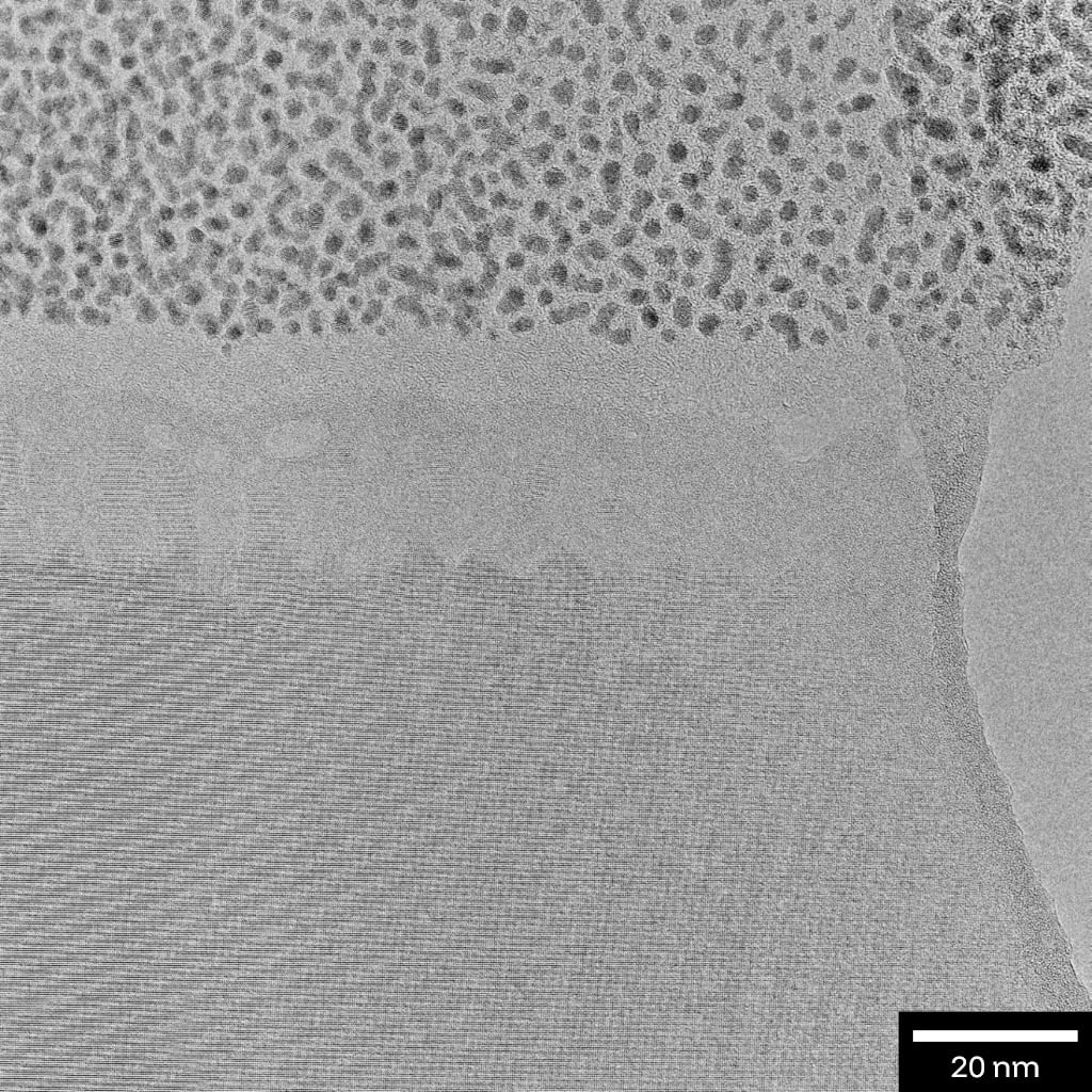
Figure 3. Ga+ FIB-polished AlN/GaN TEM specimen with Ga+ FIB-SEM (left) versus Ar+ Gentle Ion Beam-cleaned specimen (right). (Image from Technoorg Linda)
Existing Solutions, Their Limitations, and the Rationale for Full Integration of the Technoorg Aura™ Gentle Ion Beam into Tescan Ga+ FIB-SEMs
Traditional Argon Cleaning with Standalone Systems: Known and Proven Solution, Sub-Optimal Workflows
Low‑energy Ar+ ion cleaning is a well‑established method for removing FIB‑induced damage. This is not new, and the benefits are well understood. The real issue was never argon itself or that final low keV cleaning would not deliver excellent results - it was how Ar+ cleaning was traditionally implemented in the workflow.
Conventionally, Ar+ ion polishing is done as a separate, standalone step using an external ion mill. This fragmented workflow has two fundamental challenges:
- It required two separate tools - a FIB‑SEM and an Ar ion mill - which increased complexity, operator reliance, and setup time due to additional equipment, training, software, services, and even space requirements.
- Second, Ar polishing lacked real-time feedback and in-situ control of lamella quality during and after the Ar cleaning. Over-thinning and artifacts caused by standalone Ar cleaning due to wrong parameter setups became apparent only once inserted into the TEM, leading to costly waste of time of a TEM and additional costs related to must be redone.
Risks Associated with Sample Transfer
-
Damage to Specimen During Transfer
-
Oxidation or Contamination of Surface
-
Improper Alignment of Holder and Specimen
-
Contamination Due to Venting or Handling of Sample
Drawbacks of a Standalone System
-
Significant time required to set up the Ar+ Beam
-
Necessity to adapt to workflows and software
-
Inconsistent control over the quality of milling
-
Potential for over-thinning and Ar+milling defects like scratches and curtaining
Most crucially, the workflow involved multiple specimen transfers. Ultra‑thin lamellae were moved between systems and holders, exposed to venting, oxidation, contamination, misalignment, and mechanical damage. Each transfer step increased the risk of sample loss and reduced reproducibility.
In practice, Ar+ polishing done as a separate, standalone step leads to:
- High risk of lamella damage during transfers
- Oxidation and surface contamination from venting
- Misalignment between holders and systems
- No control on the thinning process in the standalone Ar Gentle Ion Mill and whether Ar‑milling is causing artifacts (e.g. curtaining, bending, etc.)
- Significant time lost to the setup of the standalone instrument and handling the same through different holders
In summary, Ar cleaning on a standalone system works—but is inherently risky, inefficient, and produces an outcome that is neither reliable nor usable by all. What needed to change was not the physics of argon milling, but its integration, control, and execution within the lamella preparation process.
Solving the Problem: A Fully Integrated Workflow with Tescan FIB-SEM Aura™ GIB Integration
The limitations of traditional Ar cleaning all came down to one issue: fragmentation. (1) Separate tools, (2) separate vacuum environments, (2) blind processing, and (3) risky sample transfers turned a proven technique into an unreliable workflow.
Tescan FIB-SEMs, for the first time, solve this by fully integrating gentle ion polishing directly inside the FIB‑SEM as hardware and are operated from a unified workflow-driven software. With AMBER 2 and SOLARIS 2, the Aura™ Gentle Ion Beam (GIB) is integrated into a single, unified ecosystem. The full specimen preparation and polishing process takes place within the FIB-SEM, from the initial milling step to the final quality check using STEM-in-SEM.

Reliable by Design
Since GIB polishing happens directly in the FIB‑SEM, all transfer‑related risks are eliminated. There is no handling between systems, no holder re‑mounting, and no exposure to ambient conditions - removing the primary causes of lamella damage, misalignment, and sample loss.
Clean and Consistent Results
The closed vacuum environment prevents oxidation and surface contamination, while the integrated dedicated holder ensures perfect alignment throughout milling and polishing. The result is consistent, controlled material removal - without the variability and artifacts associated with external processing.
Faster Time to Ultra-thin Specimens, every time, every day, by every user
There is no external tool setup, no interruption to workflow, and no external software. Ar+ ion final cleaning, polishing workflow definition, inspection, and validation happen in one place. With STEM‑in‑SEM, a final specimen quality check can be performed during the polishing and also immediately before S/TEM handover, saving time and assuring confidence in future successful S/TEM analysis. No time booked on TEM is lost.
In short, AMBER 2 replaces a fragmented, high‑risk process with a single, optimized workflow - delivering confidence, speed, and precision by default.
Conclusion: From Proven Physics to Proven Workflow
Low‑energy Ar+ ion cleaning has long been recognized as an effective way to remove FIB‑induced Ga damage and improve S/TEM lamella quality. The physics was never the limitation, nor was the achievable result. The real problem resulted in how the technology was previously deployed - as a separate, standalone step disconnected from the FIB‑SEM workflow.
Traditional external Ar+ ion milling introduced fragmentation, blind processing, and high transfer risk, making outcomes highly operator‑dependent and often unreliable. In practice, this limited reproducibility, increased sample loss, and wasted valuable (S)TEM time.
By fully integrating the Technoorg Aura™ Gentle Ion Beam directly into Tescan Ga⁺ FIB‑SEMs (AMBER 2 and SOLARIS 2), these structural weaknesses are removed. Final polishing becomes an in‑situ, controllable, and verifiable step, executed entirely inside a single system, vacuum environment, and software ecosystem.
The result is not a new cleaning principle, but a new level of reliability: damage‑free lamella preparation, clean and consistent results, and faster, more confident handover to S/TEM - every time, for every user.
|
Aspect |
Traditional Standalone Ar+ Ion Cleaning |
Integrated Aura™ GIB in TESCAN FIB-SEMs |
|
Underlying Ar+ Final Cleaning principle |
✅ Low‑energy Ar⁺ ion polishing (proven, well‑known) |
✅ Low‑energy Ar⁺ ion polishing (proven, well‑known) |
|
System configuration |
❌ Separate external Ar+ ion mill + FIB‑SEM |
✅ Fully integrated in‑chamber GIB within FIB‑SEM |
|
Sample transfers |
❌ Multiple transfers between systems and holders with associated risks of damaging or losing sample ❌ Re‑mounting and re‑alignment required on separate holders
|
✅ No transfers — sample stays in one system for FIB-SEM sample preparation and Ar+ Final Cleaning ✅ Fully aligned and stable with integrated holder and stage |
|
Oxidation & contamination risk |
❌ High risk (air exposure during transfer) |
✅ Minimal (Ar+ cleaning in FIB-SEM high vacuum chamber without specimen transfer) |
|
STEM in SEM thinning Process control and specimen quality monitoring |
❌ Polishing done “blind”. Difficult to monitor or correct. Only visible after TEM insertion |
✅ In‑situ, controlled polishing through STEM-in-SEM with immediate feedback |
|
Time efficiency |
❌ Higher setup time for a separate Ar+ GIB system, separate holders handling |
✅ No external tool setup, no workflow interruption, Simple GUI in identical FIB-SEM Software environment |
|
S/TEM utilization efficiency |
❌ Higher risk of wasted S/TEM time due to failed specimen prep |
✅ High confidence before S/TEM handover |
|
User dependency |
❌ High; experience‑driven on Ar+ milling system |
✅ Reduced; workflow‑driven and reproducible, Simple GUI in an identical FIB-SEM Software environment |
References
[1]Pastewka, L., Salzer, R., Graff, A., Altmann, F., & Moseler, M. (2009). Surface amorphization, sputter rate, and intrinsic stresses of silicon during low energy Ga+ focused-ion beam milling. Nuclear Instruments and Methods in Physics Research B, 267, 3072–3075.
[2] Datasheet of Technoorg Linda GENTLE MILL: Ion beam workstation for high-quality TEM/FIB sample preparation.
Acknowledgment

Aura™ Gentle Ion Beam Integration was jointly developed by Tescan and Technoorg Linda.
Explore how integrated FIB-SEM and ion beam workflows can support your sample preparation. Fill in the form below to connect with our team.
On-Demand Webinar Reproducible Ultra-Thin TEM Lamellae with AMBER™ 2 & Aura™

Tescan Aura™ Gentle Ion Beam (GIB)
