
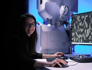
Ultra-high-resolution SEM is scanning electron microscopy designed to resolve extremely fine surface and material features at the nanoscale, including at low landing energies where surface sensitivity can be improved.
Listen to article
Why Is Ultra-High-Resolution SEM Important for Materials Characterization?
Research and development efforts in fields such as battery technology, metallurgy, and advanced materials science rely on high-resolution imaging not as an end goal, but as a critical enabler for solving complex challenges. Whether it‘s identifying nanoscale defects in metal alloys, understanding degradation mechanisms in battery electrodes, or characterizing intricate material structures, the demand for detailed, reliable data is greater than ever.
As analytical techniques become more sophisticated, the challenge is clear - how can we deliver advanced imaging capabilities without imposing unnecessary complexity on researchers? This challenge led to the development of Tescan MIRA XR, a system designed to deliver nanoscale insights without complexity, making high-resolution SEM imaging and EDS analysis accessible to all users, regardless of their level of expertise.
How MIRA XR Simplifies Ultra-High-Resolution SEM Imaging?
For decades, Tescan MIRA is a trusted name in the world of analytical FEG SEM, recognized for its ease of use, reliability, and analytical versatility. However, as research and industrial applications demand ever-higher resolution, conventional FEG SEM technology reaches its limits. At the same time, ultra-high-resolution SEM (UHR SEM) systems have traditionally been associated with multi-detector configurations that may be perceived as unnecessary by some higher throughput applications.
Tescan MIRA XR offering enhanced resolution and surface sensitivity while maintaining the intuitive operation and automation that users expect from the MIRA platform. Positioned between Tescan MIRA and Tescan CLARA, it delivers UHR imaging capabilities for industrial and research environments that value extended resolution, high throughput and streamlined operation.
To achieve this, we introduced innovations that simplify high-resolution imaging while maintaining the flexibility and precision requiring Ultra High Resolution:
-
BrightBeam™ Technology with Single High-Efficiency Axial Detector – A field-free imaging solution that enhances surface sensitivity and delivers high-quality imaging of beam-sensitive and magnetic samples without the need for surface coating. The integrated Axial detector ensures uniform signal collection, providing accurate and repeatable data across a wide range of materials and applications.
-
Apertureless Column Design – This feature eliminates the need for manual aperture selection and adjustment, ensuring optimal imaging conditions with minimal user intervention. Traditionally, SEM users needed to develop a deep understanding of aperture settings to optimize resolution, depth of field, and beam current for different sample types. With MIRA XR, can focus entirely on their research objectives, making the system more accessible and less intimidating for new and occasional users.
-
In-Flight™ Automated Controls – Automated optimization of key imaging parameters, including focus, stigmation, and beam alignment. With a single click, users can achieve sharp, high-resolution images, reducing the learning curve and accelerating data acquisition, even for complex workflows.
-
Dual Essence™ EDS Integration – A fully integrated elemental analysis solution within the SEM interface that allows for real-time compositional mapping without switching between platforms. The dual-detector setup eliminates shadowing effects, providing more comprehensive data acquisition and enhancing workflow efficiency for elemental analysis.
These innovations position MIRA XR as a high-performance SEM system that meets the demands of modern research environments by providing the resolution, flexibility, and ease of use required to tackle the most challenging materials characterization tasks.
How Automated SEM Workflows Improve Analysis Efficiency
A common perception among researchers and industry professionals is that achieving high resolution in scanning electron microscopy requires significant time investment - mastering intricate system settings, manually fine-tuning parameters, and navigating through several interfaces. In many laboratories, users face the challenge of balancing the need for high-resolution imaging with the urgency of delivering results, especially in fast-paced environments such as quality control and failure analysis.
Traditional SEM workflows often introduce inefficiencies, requiring users to switch between multiple software interfaces for imaging and elemental analysis. This fragmentation not only disrupts the workflow but also increases the time spent on sample characterization, creating bottlenecks in research and production processes.
MIRA XR addresses these challenges by simplifying the workflow and making high-resolution imaging more intuitive and accessible, reducing the perceived complexity often associated with advanced SEM systems. With the integration of Dual Essence™ EDS, users can perform real-time elemental mapping within the same live window used for imaging. This smooth integration eliminates the need to switch between platforms, minimizing distractions and ensuring continuous focus on sample analysis. Consequently, laboratories can achieve up to 30% faster analysis times, significantly enhancing throughput while maintaining the highest data quality standards.
The Wide Field Optics™ feature transforms sample navigation by enabling users to quickly and efficiently move across large sample areas, zoom in on key regions of interest, and apply automated imaging adjustments without the need to toggle between low-resolution camera navigation and SEM views. This intuitive experience not only speeds up the imaging process but also empowers users - whether novice or experienced—to achieve precise results with minimal effort.
By integrating these advanced capabilities into a cohesive and user-friendly workflow, MIRA XR allows laboratories to achieve efficiency without compromising on imaging performance. This solution adapts to the needs of both routine and research environments.
The result? Faster insights, fewer operational hurdles, and a streamlined workflow that accelerates decision-making across industries and research laboratories.
Applications of Ultra-High-Resolution SEM in Research and Industry
By addressing the complexity barrier, MIRA XR has become a valuable tool across a variety of sectors. Its versatility allows users in different fields to leverage high-resolution imaging without needing to become SEM experts. In metallurgy, the ability to analyze large, irregular samples without compromising resolution is essential for both defect analysis and quality control. In many industrial settings, quality assurance engineers frequently encounter unexpected material defects and rely on fast, accurate analysis to make critical decisions. Whether identifying inclusions, voids, or micro-cracks, MIRA XR provides the capability to quickly respond to unplanned investigations, helping labs determine „what it is“ with minimal delay. MIRA XR’s large chamber capacity and automated functions make it possible to examine multiple larger samples efficiently, ensuring that manufacturers can maintain production standards without extensive downtime. The system’s high-resolution imaging capabilities allow for detailed defect characterization, whether in bulk materials, welds, or coatings, providing the insights necessary to prevent costly failures and ensure compliance with stringent quality requirements.
Fractography is another critical aspect of metallurgy, where understanding failure mechanisms such as fatigue striations, brittle fractures, or ductile failure patterns is key to improving material performance. MIRA XR offers the necessary resolution and contrast to analyze fracture surfaces in fine detail, providing engineers with the data needed to determine root causes and implement corrective actions effectively. The system’s intuitive automation tools further enhance productivity by streamlining the imaging process, allowing users to rapidly capture and interpret complex failure features without extensive SEM expertise. With its robust analytical capabilities, MIRA XR serves as a powerful and accessible solution for metallurgical applications, ensuring that manufacturers and researchers can rely on fast, accurate results to maintain product integrity and support continuous process improvement.
How Does Low-Voltage SEM Improve Nanomaterials Characterization?
For nanomaterials research, MIRA XR’s apertureless column, BrightBeam™ technology, and automated alignments provide researchers with a reliable tool to obtain high-resolution images of sub-10 nm features with minimal manual adjustments. Achieving such precision requires the use of low landing voltages, which are essential for resolving the finest details due to the increased electron transparency at these energy levels. Traditional SEM systems often struggle to provide sufficient resolution at low keV, making it challenging to accurately characterize nanoscale structures without sample preparation techniques that can alter their properties.
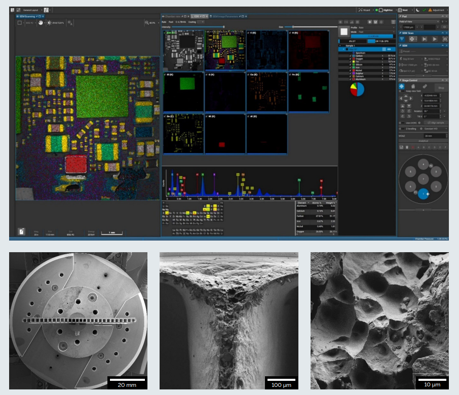 Figure 1: a) Essence™ software interface, which operators use to control Tescan Dual Essence™ EDS, displaying an impressive 17 mm FoV EDS map acquired in approximately 1 minute. (b), (c), (d) Set of images demonstrating how the software enables seamless navigation across the entire fractured sample, allowing users to efficiently identify regions of interest and final fractures within the bulk sample scale.
MIRA XR overcomes this challenge with BrightBeam™ technology, a field-free imaging solution that enables accurate imaging of beam-sensitive materials without the need for surface coating. This is particularly critical in nanomaterials research, where coating is not an option, as it can significantly alter the sample’s dimensions and obscure critical structural features. By eliminating the need for conductive coatings and providing excellent resolution at low voltages, MIRA XR ensures that researchers can observe materials in their native state with true dimensional accuracy and high contrast, supporting in-depth structural and compositional analysis.
How Is High-Resolution SEM Used in Metallurgy and Failure Analysis?
In battery research, the ability to accurately analyze the degradation of electrodes is critical to improving energy storage performance and longevity. MIRA XR provides a powerful solution for examining battery electrodes previously polished using ion milling, enabling researchers to clearly differentiate between micro and nanoscale cracks in cathode materials. This distinction is crucial for understanding failure mechanisms, as micro-cracks can propagate over time, leading to performance degradation, while nanoscale defects provide insights into material stability and processing efficiency.
MIRA XR’s high-resolution imaging and automated workflows make it an ideal system for comprehensive battery material analysis, allowing researchers to quickly obtain accurate data without complex adjustments. The system is also highly effective in the automated analysis of raw cathode and anode powders, providing detailed morphological insights that are essential for optimizing particle size distribution and uniformity. By leveraging the system’s intuitive interface and automated analysis capabilities, battery developers can streamline their workflow, accelerating research and development cycles without compromising data quality.
As a true workhorse for battery research, MIRA XR offers the flexibility to handle a wide range of sample types, from pristine materials to aged and degraded components, providing actionable insights that help improve battery design and manufacturing processes. Its robust chamber design accommodates various sample sizes and geometries, while features such as BrightBeam™ technology allow for imaging delicate electrode materials without the need for surface coating, preserving the sample’s native state for accurate characterization.
Whether supporting materials development, failure analysis, or quality control, MIRA XR empowers battery researchers with the tools they need to make informed decisions and drive innovation in energy storage technology.
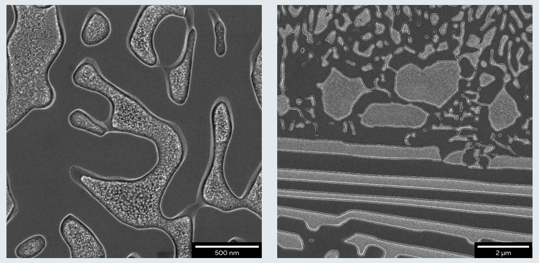 Figure 2: high-resolution surface contrast (SE) image of different phases in electron beam welded steel, acquired by in column (Axial) detector at 1 keV.
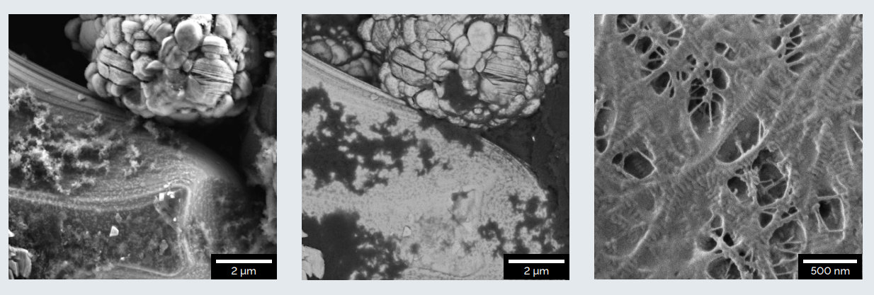 Figure 3: High-resolution surface contrast (SE) image (left) and material contrast (BSE) image (middle) of NMC powder, acquired by in-column (Axial) detector in different setups at 5 keV, and high-resolution surface contrast (SE) image of PP battery separator, acquired at 400 eV with in-column (Axial) detector in Beam Deceleration Mode (right).
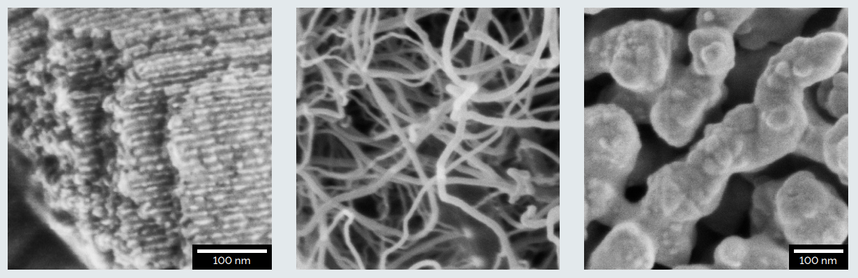 Figure 4: High-resolution surface contrast (SE) image of Mesoporous Silica (SBA-15) (left) acquired with in-column (Axial) detector at 800 eV with Beam Deceleration Mode, high-resolution surface contrast (SE) image of Carbon Nanotubes (middle) acquired with in-column (Axial) detector at 1 keV, and high-resolution surface contrast (SE) image of Nanoporous gold (right) acquired with in-column (Axial) detector at 1 eV with Beam Deceleration Mode.
How to Future-Proof High-Resolution SEM Workflows
As industries continue to evolve, so must the tools used to support their research and production efforts. MIRA XR is designed with scalability in mind, allowing users to expand capabilities with additional detectors, automation features, and software enhancements as their requirements grow.
Furthermore, MIRA XR’s long-term relevance is ensured by its ability to handle a wide variety of samples - including magnetic, large, and beam-sensitive materials - without requiring extensive preparation or adjustment. Whether in academia, R&D, or production environments, MIRA XR provides the flexibility needed to adapt to future challenges.
MIRA XR meets this need by offering:
-
Ultra-High-Resolution Imaging – Delivering the resolution required for demanding tasks in materials science, quality control, and failure analysis, without added complexity.
-
Streamlined Detection System – Featuring a single high-efficiency axial detector, MIRA XR simplifies the imaging process while ensuring reliable material contrast and high throughput, making it ideal for environments where speed and consistency are key.
-
Scalability for Future Expansion – With a modular design and multiple chamber ports, MIRA XR provides the flexibility to integrate additional analytical tools, ensuring long-term value as research requirements evolve.
-
User-Friendliness and Automation – Intuitive software and automated controls empower users of all experience levels to obtain high-quality results efficiently, reducing the learning curve and enhancing productivity.
By focusing on delivering high-performance imaging with a simplified workflow, MIRA XR provides an ideal alternative for labs seeking ultra-high resolution SEM capabilities and streamlined operations. It offers a robust and scalable platform that ensures consistency and efficiency, making it a valuable tool for ultra high resolution routine and analytical tasks.


Related Resources
Tescan MIRA XR
Ultra-high-resolution SEM for advanced materials analysis.

MIRA XR On-Demand Webinar
See high-resolution SEM and analytical workflows in action.