WEBINAR | Correlated Microanalytical Workflows for Particle Analysis Using Automated Mineralogy, FIB-SEM and SIMS

Beyond Conventional Materials Science: Design, Create and Analyse Next Generation Sensors and Devices 

Tescan Essence™ EBL Kit 

Essence-EBL-kit-hero-desktop-v02
Essence-EBL-kit-hero-mobile-v02

Dedicated software module for high precision electron beam nanopatterning for SEM and FIB-SEM

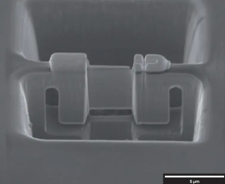
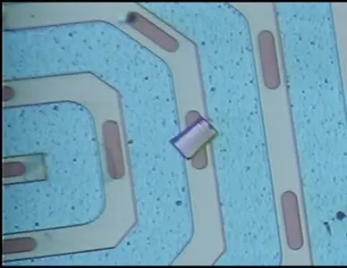
Electron beam lithography (EBL) uses a focused electron beam to draw patterns on a resist-coated surface (covered by an electron-sensitive film). It’s widely used for prototyping micro- and nanostructures with precise shapes, dimensions, and material compositions across various substrates, including sensors, photonics, plasmonics, spintronics, MEMS, microfluidics, and cell growth surfaces. 

The Tescan Essence™ EBL Kit works with Tescan’s fast electrostatic beam blanker to deliver a fully integrated EBL solution on a standard SEM. When installed on a FIB-SEM, it enables combined electron and ion beam lithography for advanced research.

  • Seamless SEM integration: The fully integrated Essence™ EBL software module works within the familiar Tescan Essence™ interface, so there’s no need for separate equipment or complex setup, just a smooth extension of your existing workflow.


  • Designed for real-world research: Supports a wide range of applications, from photonics and NEMS/MEMS to microfluidics and cell growth surfaces.


  • Precision without complexity: Z-leveling through beam refocusing, proximity error correction through fracture-free exposition for accurate and reproducible patterning.


  • Efficient from design to exposure: Avoid field stitching errors and exposure defects by tailoring your EBL exposure strategy during multifield exposures. 

Where Tescan Essence™ EBL Kit Makes the Difference

Integrated EBL Workflow  

  • Perform EBL directly on a Tescan SEM and FIB-SEM systems.

  • Use the EBL kit directly within the familiar Essence™ software GUI.

  • Combine with FIB-based lithography for multipurpose nanoprototyping. 

Flexible Pattern Design 

  • Supports mixed technologies: EBL, UV lithography, and direct write laser lithography. 

  • Full compatibility with GDSII hierarchical data format.

Exposure Optimization

  • Z-leveling through beam refocusing compensates for sample tilt. 

  • Technical layers are used to set up write field positions, reducing stitching errors in critical features. 

  • High-speed high speed patterning engine for fast and accurate exposures. 

  • Beam current control and spot size estimation optimize conditions. 

  • Proximity error correction for high fidelity patterning.

Planning Tools 

Offline exposure time simulation for better time management and instrument scheduling.

Advanced Performance

Tescan-Orage-2-MS-IMG-03

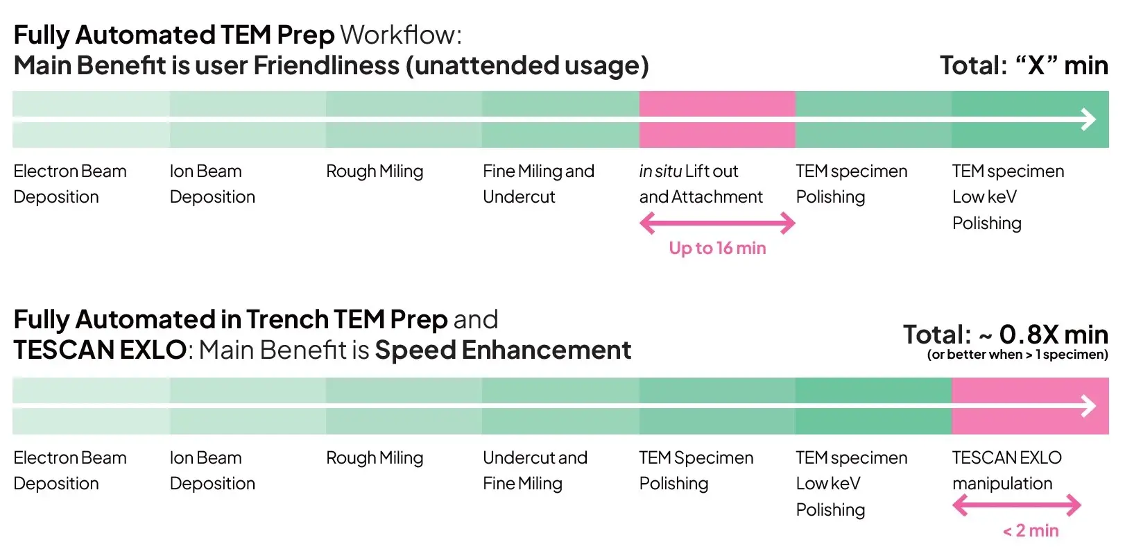
AI-powered automated workflow

The AI-driven automated lamella preparation reduces human error, shortens training time, and enables reliable unattended operation. The automation is realized through the TEM AutoPrep™ Pro software module and the OptiLift™ nanomanipulator, forming a fully integrated system that delivers fast lamella preparation while ensuring consistent quality.

Tescan-Orage-2-MS-IMG-012

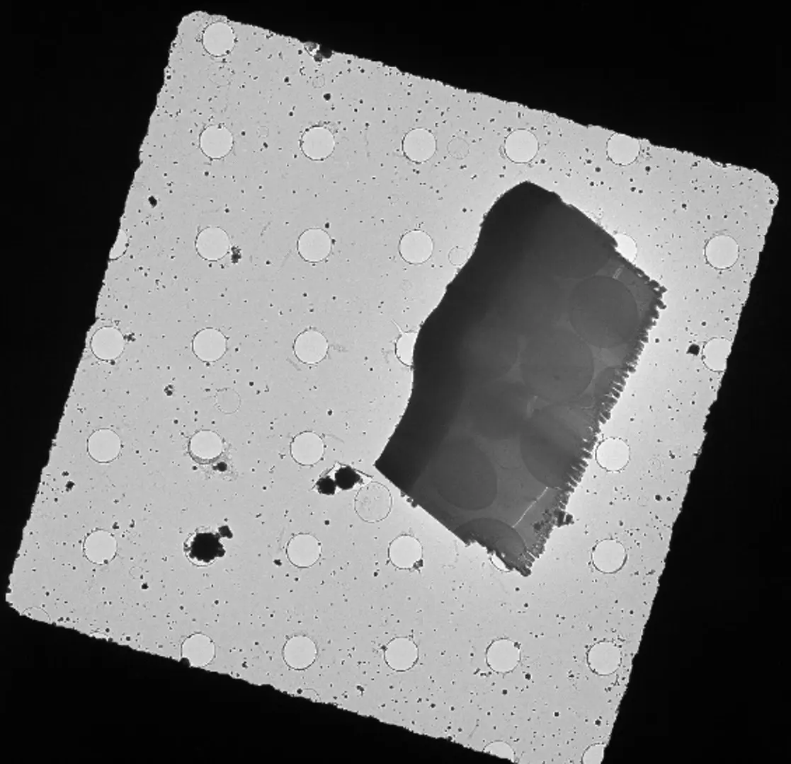
Ultimate quality of TEM lamellae 

A fully integrated Aura™ Gentle Ion Beam enables precise final polishing and gentle low-keV Ar⁺ cleaning of TEM lamellae directly inside the AMBER 2 FIB-SEM, minimizing amorphous damage and surface Ga+ contamination.

This built-in solution provides direct, real-time control over the polishing process, ensuring the highest sample quality and optimal results in TEM lamellae preparation, even for the most challenging materials. 

Unlocked content


Tescan Orage 2 APPLICATION EXAMPLES


[application examples in few words]


Unlock Tescan insight

leave a contact to access

Get the most out of Tescan

This is more than information; it's an advantage. We've compiled our technical whitepapers, detailed product flyers, and on-demand webinars to provide you with the knowledge that makes a real difference. Sign up now to access the insights you need to make an impact.

Tescan Nanomanipulator

Technical highlights
Compatible with all Tescan FIB-SEM systems

X, Y, and Z axis manipulation

Reliable in-situ TEM lamella lift-out

Smooth, low-vibration performance

Easy probe tip replacement using the removable arm

Compatible with all Tescan FIB-SEM systems

X, Y, and Z axis manipulation

Reliable in-situ TEM lamella lift-out

Smooth, low-vibration performance

Easy probe tip replacement using the removable arm

add ons (4)

GET IN Touch

with specialist

map

Where you can find us:

Tescan Brno
Libušina třída 21
623 00 Brno
Czech Republic


info@Tescan.com 

130405923 us US 37.09024 -95.712891 25.3575 29.349345 20.67957527 42.082797 39.91384763 -33.693421 13.93320106 3.039986586 31.997988 38.050985 47.579533 30.052597 48.1485965 58.375799 54.663142 19.195447 56.975106 47.916997 50.493053 45.868592 10.79556993 44.35660598 43.2371604 55.536415 14.557577179752773 32.100937 -6.116829 -6.212299277967318 33.600194 -12.08688 23.7104 -33.471062 31.998740087 -23.69149395 43.462349 51.529848 49.1893523 49.197486 25.072375 31.075811 1.299027 40.676979 52.30150662 51.013813 35.684121 37.566531 52.246622 40.581349 39.911632 -26.1811371 41.818215 33.429928

No distributors found.