Tescan’s participation will feature three highlights: its integrated semiconductor failure analysis workflow, a technical forum presentation on gas-assisted femtosecond laser sample preparation, and the interactive SPIN. MATCH. ENJOY. booth activity.
Tescan at the Event
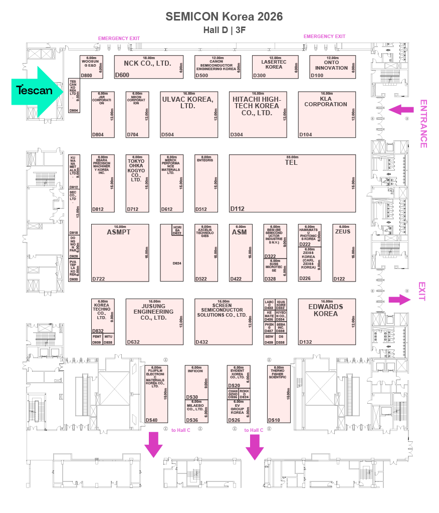
September 2–4, 2026 | Booth R8201, 4F, TaiNEX 2
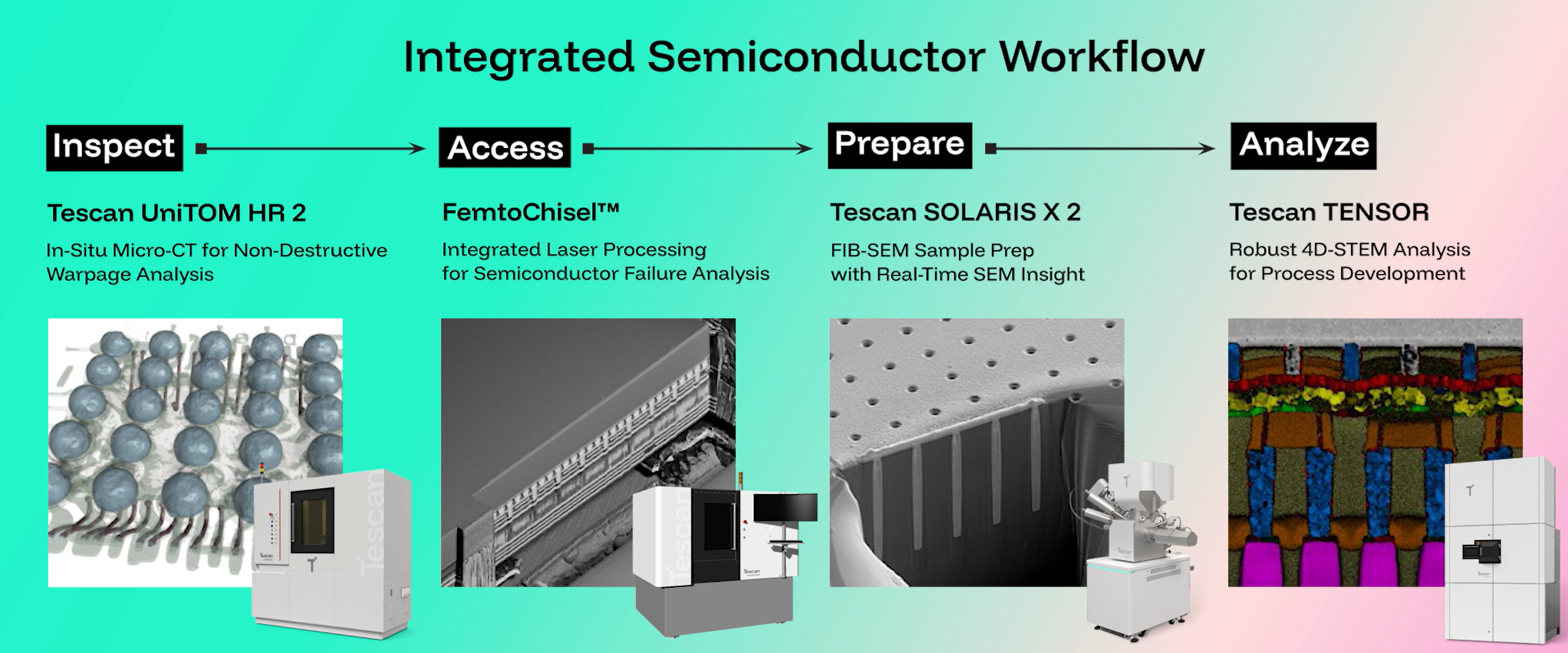
Explore a correlative workflow that connects non-destructive micro-CT inspection, femtosecond laser access, plasma FIB-SEM sample preparation, and 4D-STEM analysis. The workflow follows four stages - Inspect, Access, Prepare, and Analyze - to support defect localization and reliable downstream characterization across multiple scales.
September 2-3, 2026 | From 10:00 | Booth R8201
Spin the wheel, match each Tescan technology with its signature drink, and discover its role in the semiconductor workflow. The activity provides a concise introduction to non-destructive inspection, laser access, and FIB-SEM sample preparation, with Tescan specialists available to discuss each stage.
September 4, 2026 | 15:05–15:30 | Room 402, 4F, TaiNEX 1
Presentation: Tescan FemtoChisel™: From Hours to Minutes: High-Throughput Gas-Assisted Femtosecond Laser Workflows for Advanced Semiconductor Analysis and Characterization
Speaker: Dr. Herve Mace, Semiconductor Solution Sales Development Director

What You Will Learn
- Where micro-CT, femtosecond laser processing, plasma FIB-SEM, and 4D-STEM fit within the Inspect → Access → Prepare → Analyze workflow.
- How in-situ micro-CT supports non-destructive internal inspection and warpage analysis before physical sample preparation.
- How gas-assisted femtosecond laser processing supports cross-sectioning, decapsulation, delayering, cavity preparation, and large-volume material removal.
- How real-time SEM-guided FIB-SEM preparation and 4D-STEM analysis support site-specific preparation and downstream characterization.
Why Attend
The exhibition and forum provide complementary perspectives on semiconductor failure analysis: an integrated workflow across multiple length scales and a focused technical session on femtosecond laser sample preparation.
Visit Tescan to compare approaches, ask application-specific questions, and discuss how these methods could fit into your current laboratory workflow.
Dr. Herve Mace
Global Business Development Director, Tescan
Dr. Hervé Macé is a Director of Business Development at Tescan GROUP and Deputy General Manager of the Laser Technologies BU (Storrs/CT/USA), with over 20 years of international experience in the field of scientific instrumentation, particularly in electron microscopy and advanced analytical technologies. Prior to joining TESCAN, he held several senior commercial and strategic roles at Applied Materials, Thermo Fisher Scientific and FEI Company, including Director of Sales for EMEA, Senior Manager for Global Semiconductor Sales, and Global Accounts Manager. Throughout his career, he has been responsible for driving business development, managing global key accounts, and leading sales and service operations in high-tech domains such as semiconductors, materials science, and life sciences.