
.jpg?width=352&name=Semicon_taiwan_(8).jpg)
At SEMICON Taiwan 2026, Tescan presented an integrated failure analysis workflow designed to address the challenges of advanced packaging, heterogeneous integration, and high-bandwidth memory. The workflow connects non-destructive Micro-CT inspection, gas-assisted femtosecond laser processing, Plasma FIB-SEM sample preparation, and 4D-STEM analysis to help laboratories move from buried defect localization to reliable insight with greater speed and confidence.
Over three days, discussions at the Tescan booth explored how these technologies can work together across different length scales, helping laboratories access regions of interest, preserve critical sample context, and prepare high-quality specimens for downstream analysis.
From Buried Defects to Reliable Insight
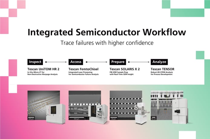
Semiconductor structures become larger and more complex, failure analysis requires more than a single instrument or technique. Buried defects must first be located without damaging the device, then accessed efficiently while preserving the region of interest for subsequent preparation and analysis.
At SEMICON Taiwan, Tescan presented an integrated semiconductor workflow that connects four stages:
-
INSPECT with Tescan UniTOM HR 2 for non-destructive Micro-CT inspection and in-situ warpage analysis
-
ACCESS with Tescan FemtoChisel™ for fast, controlled access to buried regions of interest
-
PREPARE with Tescan SOLARIS X 2 for precise Plasma FIB-SEM sample preparation supported by real-time SEM imaging
-
ANALYZE with Tescan TENSOR for robust 4D-STEM analysis
Connecting these stages helps laboratories maintain the spatial context of a defect while reducing repeated localization, sample transfers, and unnecessary rework.
From Hours to Minutes
Tescan also contributed to the Semiconductor Advanced Inspection and Metrology Forum, where Dr. Hervé Macé presented:
Tescan FemtoChisel™: From Hours to Minutes: High-Throughput Gas-Assisted Femtosecond Laser Workflows for Advanced Semiconductor Analysis and Characterization
.jpg?width=2400&height=1599&name=HPB_0928%20(1).jpg)
The presentation examined how gas-assisted femtosecond laser processing can accelerate cross-sectioning, decapsulation, delayering, cavity preparation, and large-volume material removal.
Rather than replacing FIB-SEM, FemtoChisel performs rapid material removal and provides controlled access at a larger scale. Plasma FIB-SEM can then complete the final preparation and polishing steps at the micrometer and nanometer scales.
This combination improves overall preparation throughput while helping preserve the surface quality and structural integrity required for subsequent high-resolution characterization.
.jpg?width=1200&length=1200&name=Semicon_taiwan_(8).jpg)


.jpg?width=1200&length=1200&name=Semicon_taiwan_(3).jpg)
.jpg?width=1200&length=1200&name=Semicon_taiwan_(5).jpg)
.jpg?width=1200&length=1200&name=Semicon_taiwan_(6).jpg)
.jpg?width=1200&length=1200&name=Semicon_taiwan_(7).jpg)
.jpg?width=1200&length=1200&name=Semicon_taiwan_(9).jpg)
.jpg?width=1200&length=1200&name=Semicon_taiwan_(10).jpg)
Discussing HBM and Advanced Packaging with DIGITIMES Asia
During SEMICON Taiwan, Dr. Hervé Macé joined DIGITIMES Asia for an interview about the failure analysis challenges created by high-bandwidth memory, heterogeneous integration, and advanced packaging.
The discussion explored why defects buried within complex three-dimensional semiconductor structures are increasingly difficult to locate and access. It also explained how an effective workflow combines non-destructive defect localization, controlled femtosecond laser processing, and FIB-SEM preparation.
Using the right technology at the right scale allows laboratories to accelerate access to the region of interest while maintaining the sample quality needed for high-resolution imaging and analytical characterization.
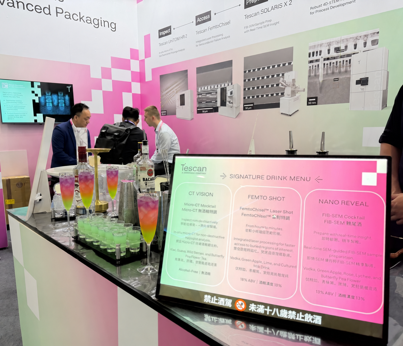
SPIN. MATCH. ENJOY.
Technical discussions at the booth were complemented by SPIN. MATCH. ENJOY., an interactive experience connecting Tescan technologies with signature drinks.
Visitors spun the wheel, matched each technology with its corresponding drink, and explored the role of Micro-CT, femtosecond laser processing, and FIB-SEM within the semiconductor failure analysis workflow.
The activity provided a different way to introduce the workflow and created opportunities for conversations around practical challenges in advanced packaging, defect localization, and sample preparation.
Most importantly, conversations with researchers provided direct insight into the questions they are asking, the limitations they encounter, and the discoveries they are working towards. This exchange helps Tescan continue developing accessible, reliable workflows around real scientific needs.
Continuing the Conversation
Tescan thanks everyone who visited the booth, attended the forum, watched the interview, or shared their failure analysis challenges with our team.
SEMICON Taiwan 2026 may have concluded, but the conversations continue. From non-destructive defect localization and large-volume material removal to precise sample preparation and nanoscale analysis, Tescan experts are ready to help laboratories identify the technologies and workflows best suited to their applications.
Trace failures with higher confidence.
Inspect. Access. Prepare. Analyze.


Related Resources
Dynamic-to-Detail Micro-CT
Explore dynamic imaging and high-resolution analysis in one workflow.

Dynamic Micro-CT Imaging
See time-resolved Micro-CT capture structural changes in 3D.

Tescan SOLARIS™ X 2
Advanced sample preparation and analysis for semiconductor workflows.