

Introduction
When selecting a scanning electron microscope, resolution is often treated as the defining parameter of performance. In practice, however, resolution specification rarely determines what you ultimately learn from your sample. What matters equally, or even more is which electrons are detected, and just as importantly, which ones are not.
When the electron beam of the SEM hits a sample, it generates a complex cloud of signals. In terms of electron signals, this cloud includes secondary electrons, originating from the very surface, and backscattered electrons coming from deeper regions of the material. The electrons are emitted at different energies and directions, and the different types of signals generated all carry valuable information, while inherently mixed together.
An SEM image is therefore not a direct representation of a sample. It is a “filtered” image generated and shaped by the detector system. If the filtering mechanism is not regulated, the result can be misleading. Surface features, compositional contrast, and additional subsurface information can overlap in ways that make interpretation difficult or even incorrect. This leads to a fundamental principle: SEM imaging is not about collecting as many electrons as possible, but about selecting the right electrons to answer specific questions about material differences, shapes and topographies.
Secondary vs Backscattered Electrons: What Each Signal Means
When the primary electron beam interacts with a sample, the two most important signals used for imaging are secondary electrons (SE) and backscattered electrons (BSE). While both originate from the same interaction spot, they are generated through different physical processes and carry fundamentally different types of information.
Secondary electrons are low-energy electrons that are ejected from atoms in the sample as a result of inelastic interactions with the incoming beam. Because they lose energy very quickly within the material, only those generated extremely close to the surface are able to escape and reach the detector. In practice, this means that the detected SE signal originates from the very top layer of the sample, typically within just a few nanometers.
This strong surface sensitivity makes secondary electrons ideal for imaging fine morphological details. Features such as edges, roughness, and small surface structures are clearly visible because the emission of secondary electrons is highly dependent on local geometry. Areas with sharp edges or higher inclination angles tend to emit more electrons, which makes them appear brighter in the image. As a result, SE images naturally emphasize topography and often appear highly detailed and almost three-dimensional.
Backscattered electrons, in contrast, originate from elastic interactions between the primary beam electrons and atomic nuclei within the sample. In this process, the incoming electron is deflected rather than absorbed, and can eventually escape back out of the material with a relatively high remaining energy. Because of this higher energy, backscattered electrons can travel longer distances within the sample, meaning that the detected signal comes from a significantly larger and deeper interaction volume.
The key characteristic of backscattered electrons is their sensitivity to atomic number. Heavier elements scatter electrons more strongly than lighter ones, resulting in a higher number of backscattered electrons reaching the detector. This creates compositional contrast in the image, where regions containing heavier elements appear brighter and lighter elements appear darker. Unlike secondary electrons, BSE signals are much less influenced by surface geometry, which makes them more reliable for distinguishing material differences.
This leads to a fundamental distinction between the two signals. Secondary electrons provide detailed information about the surface shape of the sample but carry limited information about composition. Backscattered electrons, on the other hand, provide insight into material differences and phase contrast, but with reduced sensitivity to fine surface features and typically lower spatial resolution.
Understanding this difference is critical for correct interpretation of SEM images. The same region of a sample can appear completely different depending on whether SE or BSE signals are detected. Surface features that are clearly visible in secondary electron imaging may disappear in a backscattered image, while compositional variations that are invisible in SE mode may become the dominant contrast in BSE mode. This contrast change is shown directly in Figure 1, where SE imaging reveals the NMC particle surface morphology while BSE imaging highlights compositional differences in the binder and additive phases.
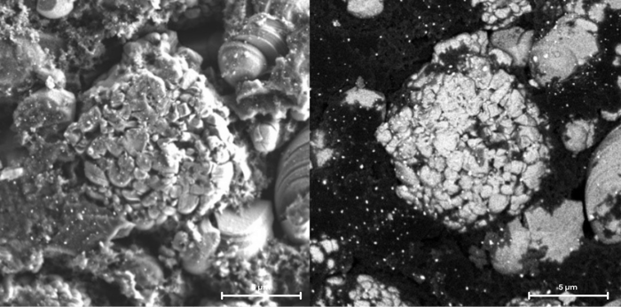 Figure 1. Comparison of secondary electron (SE) and backscattered electron (BSE) imaging of a battery cathode material. The figure shows the same region of a battery cathode imaged using two different detection modes. The left image, acquired using secondary electrons (SE), emphasizes the surface topography of the material. The morphology of the NMC particles is clearly visible, including their rough, layered surface structure and fine surface details. The binder phase appears as a smoother, less structured background, while small nanoparticles are visible but not strongly distinguished from the surrounding material due to the topography-dominated contrast. In contrast, the right image, acquired using backscattered electrons (BSE), highlights compositional differences within the same region. The primary NMC particles appear relatively uniform, while regions of different composition become more apparent. In particular, small, bright nanoparticles - identified as Ti-based additives - stand out clearly against the darker binder matrix due to their higher atomic number. The binder phase appears significantly darker, reflecting its lower atomic number (carbon) and reduced backscattered electron signal.
From a practical perspective, neither signal alone provides a complete picture. Secondary electrons tell you how the surface looks, while backscattered electrons tell you what the material is. The real understanding comes from combining both perspectives - and, as discussed in the following sections, from further controlling which parts of these signals are detected. This basic difference between elastic and inelastic electron interactions is illustrated schematically in Figure 2, which explains why SE and BSE signals carry different types of sample information.
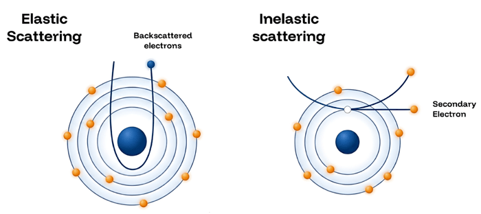 Figure 2. The schematic illustrates two fundamental interaction mechanisms between the primary electron beam and atoms in the sample. On the left, elastic scattering shows an incident electron (from SEM beam) being deflected by the atomic nucleus with minimal energy loss. As a result, the electron changes direction and can escape the material as a backscattered electron (BSE). On the right, inelastic scattering demonstrates an interaction where energy is transferred from the incoming electron (from SEM beam) to the atom, leading to the ejection of a secondary electron (SE). These electrons have low energy and can only escape if they are generated very close to the surface. This fundamental difference explains why BSE signals provide compositional information from deeper regions, while SE signals are highly surface-sensitive and reveal fine topographical details.
The Electron Cloud: Too Much Information by Default
Every interaction between the electron beam and the sample produces more information than we want to see at once. The emitted electrons differ in three key aspects: their energy, their direction, and the depth from which they originate. These differences are directly linked to different types of contrast. Surface-sensitive features are typically carried by low-energy secondary electrons, while compositional information comes from higher-energy backscattered electrons. At the same time, the angle at which electrons leave the sample strongly influences whether topography or material contrast dominates the image.
If all of these signals are collected together, the resulting image becomes a mixture of multiple effects. Bright areas may not necessarily correspond to material contrast, but instead to edge effects caused by local geometry. Similarly, deeper signal contributions can mask fine surface details. In such cases, the image may appear detailed, but the information it contains is difficult to interpret reliably. The key challenge in SEM is therefore not only signal generation, but signal separation.
Detector Placement: In-Column vs Chamber mounted
The first level of control over this signal comes from detector placement. In SEM systems, detectors are typically located either inside the chamber near the sample or within the electron column itself. This positioning directly determines which electrons can physically reach the detector.
Chamber-mounted detectors are positioned close to the sample and collect electrons emitted over a wide range of angles. Because of this, they are highly sensitive to surface geometry. Features such as edges, roughness, and structuring are strongly emphasized, resulting in images with pronounced topographical contrast. This makes chamber detectors particularly effective for visualizing morphology and navigating across a sample.
In contrast, in-column detectors are aligned with the primary beam axis and collect electrons traveling at narrow angles. These electrons are less influenced by surface shadowing effects and provide a more uniform signal. As a result, images acquired with in-column detectors tend to suppress strong edge contrast and offer a clearer representation of material-related differences. This configuration is also often associated with higher resolution capability due to shorter working distances.
A useful way to understand this difference is to consider illumination geometry. Chamber detectors behave similarly to side illumination, where shadows enhance surface features. In-column detectors, on the other hand, resemble coaxial illumination, where shadows are minimized and the image appears flatter but more uniform. Neither approach is inherently better; each emphasizes different aspects of the sample. Figure 3 demonstrates this point by comparing the same graphene and Zn nanoparticle sample with in-column and chamber-mounted SE and BSE detector configurations.
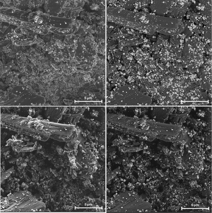 Figure 3. Comparison of graphene with Zn nanoparticles imaged using different SEM detector configurations. The figure shows the same sample area acquired with in-column SE, in-column BSE, chamber-mounted SE, and chamber-mounted BSE detectors. Each detection mode filters the electron signal differently, changing the balance between surface topography and material contrast. In-column SE emphasizes fine surface details with reduced shadowing, while chamber-mounted SE provides stronger topographical contrast. In-column BSE highlights material-related contrast with less influence from surface geometry, whereas chamber-mounted BSE combines compositional information with stronger sensitivity to local shape and shadowing. Together, the comparison demonstrates how detector position and signal type influence what is visible in the final SEM image.
Angular Filtering: Separating Directional Information
While detector placement defines the general range of collected electrons, angular filtering adds another level of control. The important point is that electrons do not leave the sample in one direction only. Some leave at low angles, close to the sample surface, while others travel more directly back toward the column. These different angular ranges carry different information.
A chamber-mounted BSE detector is positioned below the pole piece and closer to the sample. From this position, it collects a wider and often lower-angle part of the BSE signal. This makes it more sensitive to surface geometry, crystallographic orientation, and local shadowing effects. The image therefore contains material contrast, but also a stronger contribution from samples topography. This can be useful when the user wants to see how material differences relate to surface structure and topography features across the sample.
In-column BSE detection works differently. Because the detector is positioned along the optical axis, it preferentially collects electrons that travel closer to the beam direction. These higher-angle or more axial BSEs are less influenced by surface shadowing and surface inclination. As a result, the image tends to look flatter, but the material or atomic-number contrast becomes easier to interpret. In-column angular filtering therefore helps to reduce topographical interference and reveal material differences that could otherwise be hidden in rough surfaces, holes, or complex geometry.
The key message is that chamber-mounted and in-column BSE detectors do not simply provide “better” or “worse” images. They filter the electron cloud differently. A chamber-mounted detector gives a broader, more surface structure-describing view. An in-column detector gives a more axial and cleaner material-composition only related view. By comparing both, the user can separate what comes from the shape of the sample and what comes from the material differences itself. This separation is visible in Figure 4, where different BSE collection angles progressively reduce topographical influence and make the material-related contrast easier to interpret.
This is why angular filtering is not only about detector segmentation. It can also be achieved by detector geometry. When BSE detectors are placed at different positions, they naturally collect different take-off angles. The result is a set of complementary images from the same sample: one emphasizing topography and material contrast, another emphasizing material contrast with less topographical influence. This makes SEM interpretation more reliable, especially for complex samples where geometry and composition are mixed together.
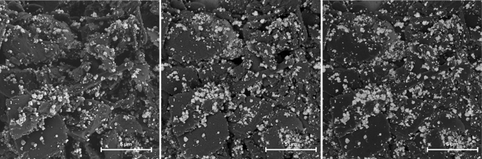 Figure 4. Angular filtering of BSE signals from graphene with Zn nanoparticles. The figure compares the same sample area imaged using three BSE detection geometries: chamber-mounted BSE on the left, mid-angle in-column BSE in the middle, and axial narrow-angle BSE on the right. The chamber-mounted BSE image collects a broader angular range, thereby combining material contrast with stronger topographical and shadowing effects. The mid-angle in-column BSE image reduces the influence of this geometry and provides a more balanced view of the material and surface-related contrast. The axial narrow-angle BSE image further suppresses topographical contribution and emphasizes cleaner material-related contrast. Together, the comparisons show how angular filtering helps separate information coming from sample shape and surface structure from information related to material composition.
Energy Filtering: Controlling Information Depth
In addition to angular selectivity, signal separation can also be achieved through energy filtering. This approach focuses on the relationship between electron energy and the depth from which the electron originates.
Electrons generated near the surface typically experience fewer interactions within the material and therefore retain higher energy when they leave the sample. In contrast, electrons originating from deeper layers undergo more scattering processes and lose a greater portion of their energy before escaping. This difference allows surface-related information to be separated from subsurface contributions.
Energy filtering is implemented by introducing an electrical bias, typically in the form of a grid placed in front of the detector. This grid acts as an energy threshold. By adjusting the bias, only electrons above a certain energy are allowed to reach the detector. Increasing the threshold progressively suppresses lower-energy electrons, effectively filtering out deeper signals and enhancing surface sensitivity.
This capability is particularly valuable when working with modern materials, where relevant features are often confined to extremely shallow regions. It allows the user to precisely control how deeply the microscope “sees” into the sample, improving clarity and reducing ambiguity in interpretation. Figure 5 shows this effect on an NMC cathode with binder, where increasing the energy threshold changes the contribution of detected electrons and tunes the image toward more selective BSE contrast.
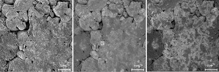 Figure 5. Energy filtering of BSE signals in an NMC cathode with binder. The figure shows the same cathode region acquired at 1 keV using an energy-filtered in-column detector. The left image shows a topography-dominated SE contrast, where surface morphology and particle structure are most visible. The middle image shows a conventional BSE contrast with low-energy electrons filtered out at 50 eV out of 1000 eV, providing material contrast view. The right image shows BSE contrast with stronger energy filtering at 700 eV out of 1000 eV, which further changes the balance of detected signal and enhances surface-related material contrast. Together, the comparison demonstrates how energy filtering controls the contribution of electrons with different energies and helps tune the image from general morphology toward more selective BSE contrast.
From Signal Mixing to Signal Control
When combined, detector placement, angular filtering, and energy filtering form a comprehensive framework for signal control. Each of these mechanisms isolates a different aspect of the electron cloud: spatial direction, emission angle, and energy. Together, they enable precise selection of the information that contributes to the final image.
Without this level of control, SEM imaging remains limited by signal mixing. Important details may be hidden, and contrast mechanisms can interfere with each other. With proper control, however, the SEM becomes a much more powerful analytical tool, capable of isolating specific types of information and delivering results that are both clearer and more reliable.
Translating Principles into Detector Design: The Tescan Approach
These principles are not only theoretical; they directly influence how modern SEM systems are designed. Tescan’s detector architecture is built around the idea that meaningful imaging requires flexible and controlled signal selection rather than a single detection path.
This is reflected in the combination of multiple detectors positioned both in the column and within the chamber. By providing more than one in-column detector, including the capability to detect backscattered electrons, the system allows simultaneous collection of signals with different angular characteristics. Chamber-mounted detectors further extend this range, enabling broad angular coverage and strong topographical sensitivity.
Energy filtering adds a further dimension of control. Available on advanced Tescan platforms, this functionality enables selective detection of backscattered electrons based on their energy, allowing users to isolate surface-sensitive information or suppress deeper signal contributions as needed.
Taken together, this combination of multiple detection geometries, angular segmentation, and energy selection provides a level of flexibility that directly addresses the fundamental challenge of signal mixing. Instead of adapting the interpretation to the image, the system allows the image to be adapted to the question.
Conclusion: From Image to Understanding
Every SEM image originates from a complex mixture of signals generated within the sample. The challenge is not in producing these signals, but in selecting the ones that are relevant. Without control over this process, images may appear detailed but remain difficult to interpret correctly.
The key to meaningful SEM analysis lies in understanding that detection is a filtering process. By controlling which electrons are detected—based on their direction, energy, and origin - it becomes possible to isolate specific types of information and significantly improve the reliability of the result.
Ultimately, the quality of insight in SEM does not depend on how many electrons are collected, but on how effectively they are selected.
The practical detector choices discussed throughout the article are summarized in Table 1, which links common imaging questions to the detector principle most suitable for isolating the relevant signal.
SEM Detector Selection Guide: Practical Decision Framework
| Use case/ question | What you need to isolate | Recommended detector principle | What you will see |
| Surface morphology (edges, roughness, particles) | Wide-angle, geometry-sensitive electrons | Chamber-mounted SE or BSE (low-angle) | Strong topography, edge contrast, shadowing |
| Material/phase contrast | Narrow-angle BSE signal (less geometry influence) | In-column BSE and chamber mounted BSE detector | Clear compositional contrast, reduced shadowing |
| Separate topography vs material contrast | Directional (angular) information | Chamber mounted Quadrant / segmented BSE (e.g. 4QBSE) In column narrow angle BSE In column mid-angle BSE |
Controlled contrast: sum = material, difference = topography |
| Surface-sensitive material contrast information (thin films, nano particles) | High-energy BSE electrons (surface-origin) | Energy-filtered BSE | Enhanced BSE surface sensitivity, suppressed subsurface signals |
| Avoid mixed or misleading contrast | Isolation of signal types | Combination of detectors (angular + energy + placement | Clean, interpretable image linked to real sample properties |
| Complex samples (geometry + composition mixed) | Multi-signal separation | Multi-detector acquisition (in-column + chamber + segmentation) | Multiple contrast modes from one dataset |
Written by Petr Klimek, PhD.
Product Marketing Director, Tescan


Related Resources
Tescan CLARA™
Maximum information from every scan and any sample at the nanoscale

SEE MORE. UNDERSTAND MORE.
Introducing the New Tescan CLARA™

Submit Your Sample for Advanced Contrast SEM Analysis
Join a Collaborative Study in Advanced Contrast SEM