
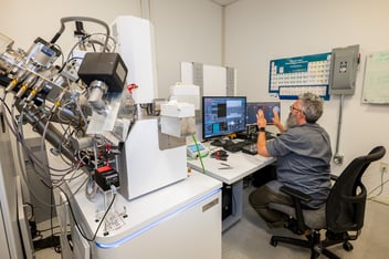
At a shared electron microscopy facility, no two days are alike. Researchers rarely arrive with the same type of sample or even the same kind of question. One may need to reveal what lies beneath the surface, while another is trying to characterize a fragile structure in its native state or understand how a material changes with depth. For the core facility team, versatility is not simply convenient. It is essential.
Meeting that variety requires more than a broad range of instruments. It also takes experience: knowing how to translate an unfamiliar sample and open-ended scientific questions into a practical preparation and characterization workflow.
Dr. Jamie Ford brings that perspective to the Nanoscale Characterization Facility (NCF) at the University of Pennsylvania. With a background in chemistry and a PhD in Materials Science and Engineering, he supports instrument maintenance and user training while helping researchers make effective use of the facility’s microscopy capabilities, including Tescan AMBER X plasma FIB-SEM (PFIB-SEM).
We spoke with Jamie about operating a PFIB-SEM in a multidisciplinary environment, the capabilities that make it suitable for such varied research needs and how its versatility helps researchers approach very different samples and scientific questions.
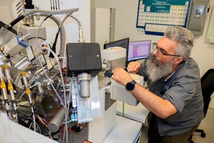 Photo credit: Sylvia Zhang
When every project is different
The Nanoscale Characterization Facility is housed within the Singh Center for Nanotechnology and supports researchers from across the University of Pennsylvania and the wider Mid-Atlantic region.
Its three-person team manages six electron microscopes. Jamie oversees the SEMs and is directly responsible for the facility’s ion beam instruments: Tescan AMBER X and a helium ion microscope.
For projects requiring FIB-SEM capabilities, the team relies on a single platform to support a wide variety of samples and workflows.
“The AMBER X is our only FIB, but it handles everything we throw at it,” Jamie says.
The applications include TEM lamella preparation for electron energy-loss spectroscopy (EELS), large trench milling for investigating subsurface cracks in dental ceramics, secondary ion mass spectrometry (SIMS) for energy materials, cryogenic preparation of biological samples and EBSD (Electron Backscatter Diffraction) analysis of buried interfaces.
In an open access facility, flexibility is essential. The team must be ready to work with a wide variety of samples, address new research questions and support very different analysis requirements.
The answer may lie beneath the surface
Despite the diversity of projects, deciding whether plasma FIB-SEM is the right tool often comes down to two practical questions: Does the researcher need to access something below the surface, and how much material needs to be removed?
When the target lies beneath the surface and the required excavation is smaller than approximately one millimeter, the sample will typically go to the PFIB-SEM. The broad current range of its Xe plasma source is particularly valuable in a multi-user environment, where milling requirements can vary considerably from one project to the next.
“The ability to mill huge trenches quickly and then fine polish at high resolution on the same platform is a wonderful experience,” Jamie adds.
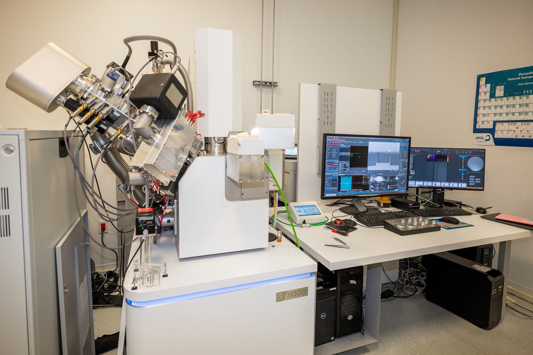 Photo credit: Sylvia Zhang
Performance matters, but so does availability
The practical benefits of AMBER X are not limited to its performance. In an open access facility, instrument availability and cost efficiency are equally important.
After almost seven years of operation, the instrument had only recently started using its second xenon tank and the first was not yet completely empty.
“This saves time and money and ensures the instrument is up and available to users the vast majority of the time,” Jamie explains.
For a busy research center, that means fewer interruptions and more consistent support for ongoing projects.
Turning shades of grey into scientific answers
For many researchers, imaging is only the starting point for understanding a sample’s composition and structure.
“An image of detected electron intensity can only tell you so much about your sample if you don’t have the background context to understand what the different shades of grey mean,” Jamie says.
This is where analytical techniques such as EDS, ToF-SIMS and EBSD complement PFIB-SEM imaging by revealing information that structural observations alone cannot provide.
EDS maps the elemental composition of the analyzed region, while ToF-SIMS provides detailed chemical information from the surface and, through depth profiling, across successive layers. EBSD reveals grain structure and crystallographic orientation and, when combined with FIB milling, can show how these features vary below the surface.
These techniques allow users to move from simply observing a feature to asking more specific questions, for example: Which elements are concentrated at an interface, how does the grain structure change below the surface, or how do metals redistribute during the annealing of a thin-film stack.
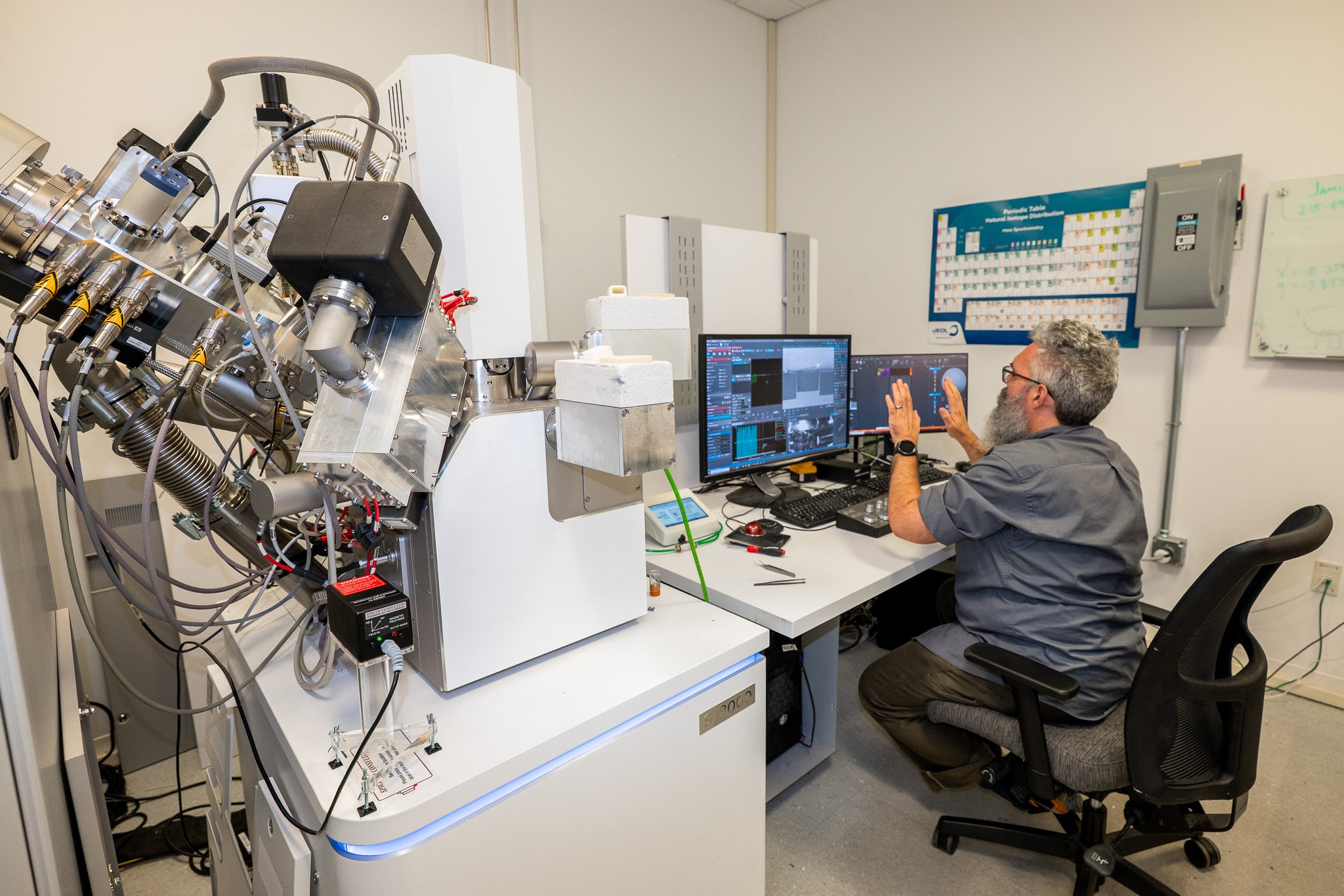 Photo credit: Sylvia Zhang
When cooling changes the picture
Some materials cannot be meaningfully studied in their native state at room temperature.
The facility’s main cryogenic workflows include the investigation of lithium–liquid-electrolyte interphases and the preparation of biological TEM samples. In both cases, maintaining low temperatures is necessary to preserve the sample in a stable, immobile state.
Jamie’s work with low-melting-point and heat-sensitive materials has also reinforced a practical lesson: when a sample behaves unexpectedly, temperature may be part of the explanation.
“If something looks weird or behaves oddly at room temperature, cool it down and try again,” he advises. “Perhaps it’ll ‘be normal’ at −150 °C.”
This approach has helped clarify some issues encountered with lithium films and GaN substrates. Cooling the specimen can reduce temperature-related artifacts, preserve sensitive structures and provide a more reliable basis for sample preparation and analysis.
A new PFIB column, a visible difference
The facility recently upgraded its AMBER X™ with the Mistral plasma FIB column. From Jamie’s perspective, day-to-day operation remains familiar, but the results are noticeably different.
“It’s very much like using the old column, but all of the milled sidewalls are nicer. Like, way nicer,” he says.
The improvement became especially apparent once the effects associated with beam tails were reduced. More clearly defined beam boundaries make milling behavior easier to predict and may be particularly valuable for automated workflows.
“Knowing where the edge of the beam is instead of kind of guessing will help a lot,” Jamie adds.
He is also continuing to evaluate the column’s low-acceleration-voltage performance, with a particular focus on understanding its effect on SIMS collection and where low-kV operation may offer the greatest value.
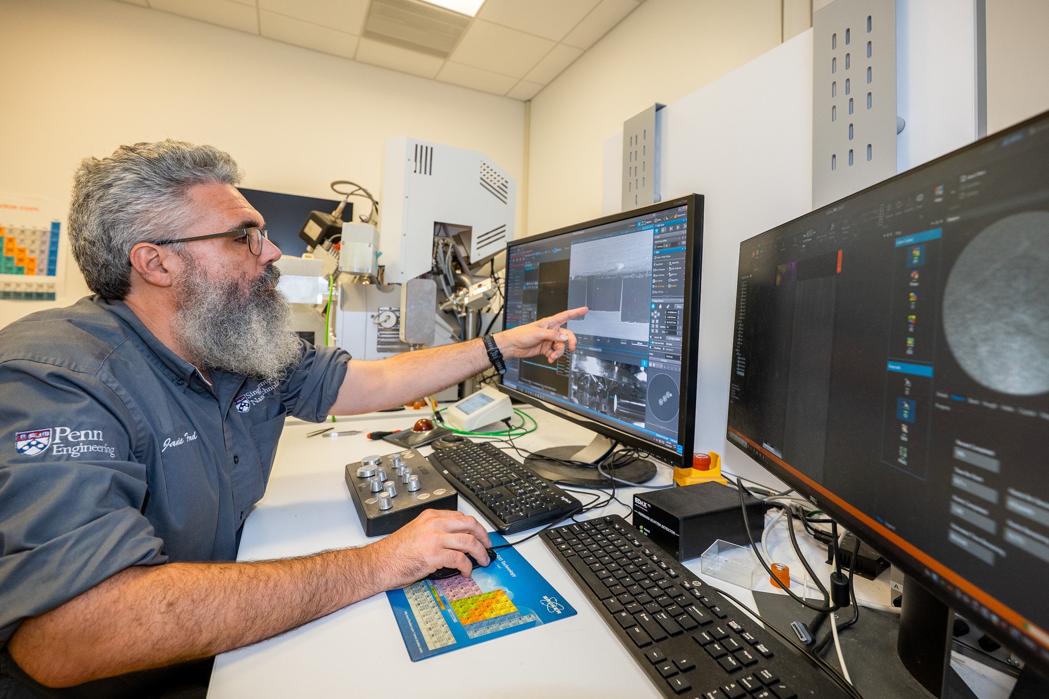 Photo credit: Sylvia Zhang
Complementary techniques, deeper insight
Some of the facility’s newest work combines multiple techniques to build a more complete picture of changes within materials.
Jamie is particularly excited about using variable-voltage SIMS to study annealed thin-film stacks. The research explores how different metals redistribute during annealing, how SIMS resolution can be maximized and how the acquired data can be correlated with FIB tomography to aid segmentation.
The facility is also exploring EBSD analysis of buried interfaces. High ion-beam currents provide rapid access to the interface, after which the exposed region can be polished gently and reliably for crystallographic characterization.
These workflows show how plasma FIB-SEM can become more than a tool for material removal and specimen preparation. By combining milling and imaging with complementary analytical data, researchers can interpret their observations with greater confidence.
Start with the sample and stay curious
For researchers planning their first plasma FIB-SEM experiment, Jamie’s advice is refreshingly direct: “Put your sample in the instrument and see what you see.”
Initial observations often lead to new questions, which can then be explored through further milling, imaging or analytical characterization.
“You don’t know what you don’t know until you don’t know it,” Jamie adds, offering an important reminder that scientific discovery often begins by recognizing the limits of what we already understand.
In an open user facility, this willingness to explore is paired with the ability to follow unexpected findings. Whether the challenge involves a large ceramic trench, a frozen biological specimen, an energy-material interface or a nanoscale chemical distribution, plasma FIB-SEM provides a flexible route from the first observation to a deeper understanding of the sample.
Written by Kateřina Němcová
Content Marketing Specialist, Tescan


Related Resources
Tescan AMBER™ X 2
Plasma FIB-SEM for advanced research workflows.

Advanced APT Workflows
See how plasma FIB-SEM improves APT preparation.

AMBER™ X 2 in Research
See how researchers use AMBER™ X 2 in practice.