
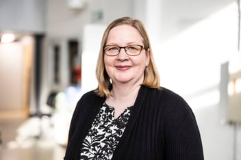
Every tool, engine, and moving part eventually wears down. But what actually happens at the surface, where materials meet, rub, and slowly break apart? Answering that question is the daily work of Dr. Kati Valtonen, Staff Scientist at Tampere University, where electron microscopy turns invisible wear processes into insight that helps materials last longer. Working alongside researchers and industry partners, she connects what happens at the microscale to how materials perform in the real world.
When she first started working with electron microscopes more than 30 years ago, Kati Valtonen could hardly have imagined the capabilities available today. Her work sits right at that surface, where friction, wear, and deformation quietly reshape materials over time. Across coatings, failure analysis, and wear-resistant materials, she has spent her career reading the small-scale clues that explain why materials succeed or fail in service and helping industry partners act on her findings.
In this interview, she takes us inside Tampere University's materials science research and onto the Tescan CLARA™ scanning electron microscope, from in situ micromechanical testing and EBSD mapping to nanoindentation and low-voltage backscattered-electron imaging, showing how each helps observe materials deform and wear, and reveal their hidden structure.
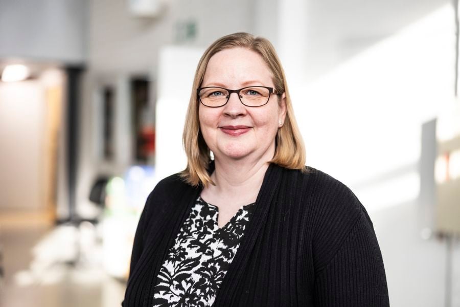
Career Path: From Failure Analysis to Wear Research
Before we meet the scientist, a quick word on the field itself. Wear research asks how materials degrade in service, whether through abrasion, the wearing away caused by scraping and rubbing, or erosion, the loss caused by particles or fluids striking a surface. Reading those small-scale changes is how Dr. Valtonen predicts how a component will hold up in the real world.
Q: Could you briefly introduce your role at Tampere University and what the Tampere Wear Center focuses on?
"As a Staff Scientist, I am responsible for the research infrastructure of the Tampere Wear Center and the materials characterization facilities within Engineering Materials Science at Tampere University. My work combines scientific, technical, and educational responsibilities. In practice, I provide user training for advanced characterization equipment, support researchers in planning and conducting wear experiments, facilitate microscopy studies, coordinate infrastructure development and procurement projects, and serve as a key contact person for industrial partners.
Education is also an important part of my role. I lecture on optical and scanning electron microscopy and microanalysis at the bachelor’s level and teach abrasion and erosion wear mechanisms at the master’s level. Working with students at different stages of their studies allows me to share practical expertise while encouraging the next generation of materials scientists and engineers."
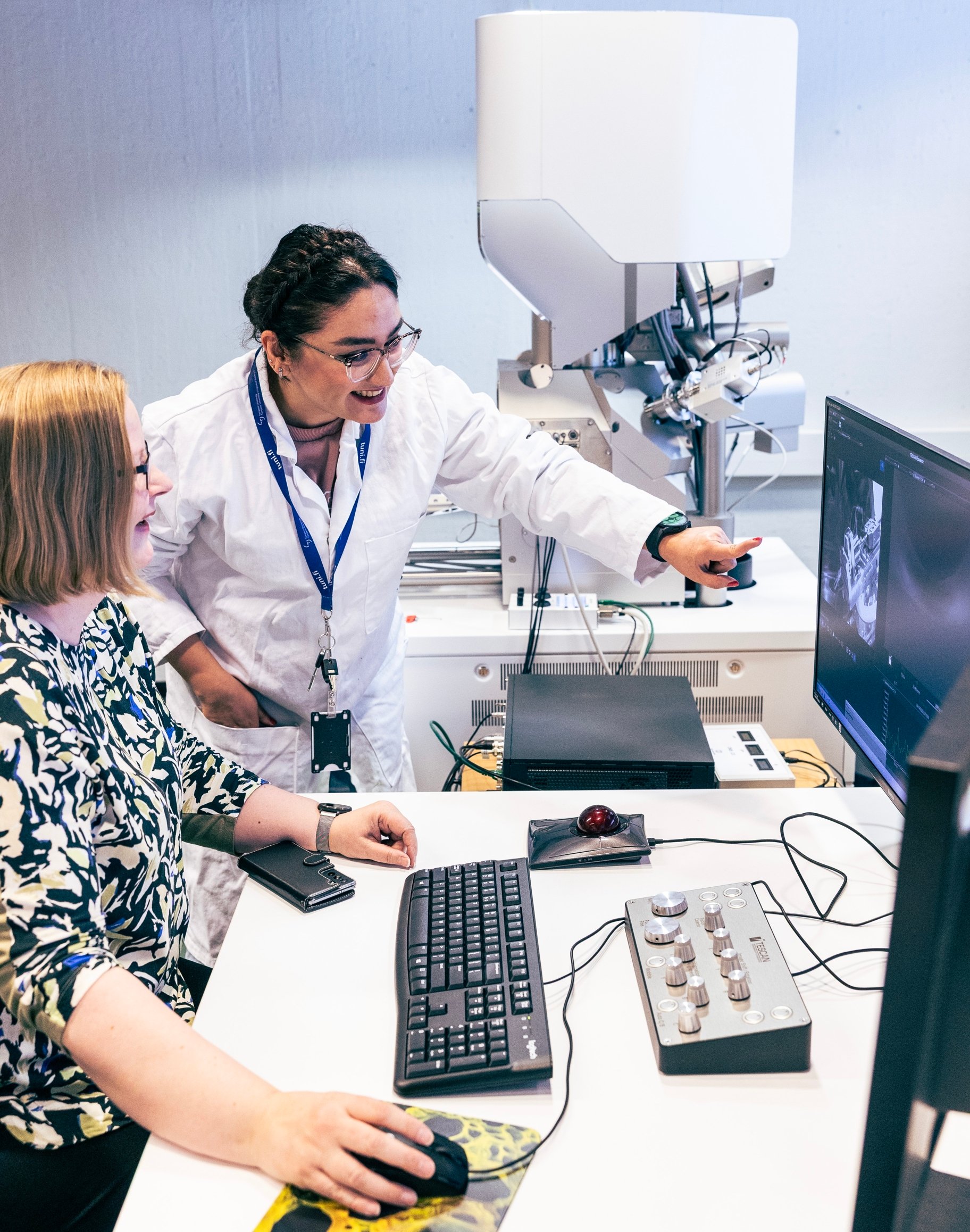 Dr. Valtonen training Doctoral Researcher Bahareh Javanpour.
Her path runs through the science of tribology, the study of what happens when surfaces meet and move against one another, caught between friction, wear, and lubrication. It is a field she came to by way of some unexpected turns.
Q: Your career spans multiple areas, from electron microscopy and paperboard coatings to tribology. Could you tell us about your research career?
"Electron microscopy has been at the core of my research career for more than 30 years. I began with small industrial projects focused on failure analysis, using microscopy to investigate the root causes of material failures.
Later, my research concentrated on the characterization of water-based paperboard coatings, where I combined scanning electron microscopy (SEM), X-ray diffraction (XRD), and atomic force microscopy (AFM) to study coating structures and properties."
Much of that curiosity centers on the traces wear leaves behind. As a material is worn, thin surface layers known as tribolayers build up, holding a record of the friction, deformation, and abrasive contact the surface has endured. Learning to read them is where her fascination with wear truly took hold.
Q: What inspired your interest in material wear, and were there key moments that steered you toward this field?
"A significant turning point in my career came in 2008 with the establishment of the Tampere Wear Center, where I joined as a project manager. Working closely with material development projects for the mining and mineral processing industries sparked my interest in wear-resistant materials and inspired me to pursue a PhD. My doctoral thesis, 'Relevance of Laboratory Wear Experiments for the Evaluation of In-Service Performance of Materials,' examined how laboratory wear tests can be used to predict the actual performance of materials.
Throughout this work, SEM played a crucial role in characterizing wear surfaces and tribolayers formed during service. Tribolayers are particularly challenging to study because wear processes impose severe deformation on surface materials, resulting in complex nanostructured layers. Characterization of these layers is essential for understanding wear mechanisms and ultimately improving material performance in demanding industrial applications."
The Tescan CLARA in Practice: In Situ Testing, EBSD, and Nanoindentation
What makes an instrument like the CLARA so powerful is the chance to watch materials in the act. In-situ work lets Dr. Valtonen's colleagues follow a material as a process unfolds in real time, while operando studies push further still, observing it hard at work under genuine operating conditions rather than in an isolated test.
Q: How does the Tescan CLARA fit into your research, and which capabilities have proven most useful so far?
"A major focus of our research with the Tescan CLARA scanning electron microscope is the study of deformation behavior at small length scales. We use in situ micromechanical testing inside the SEM to investigate how materials respond to mechanical loading under a wide range of conditions. The current setup enables the combination of electron backscatter diffraction (EBSD) mapping and nanoindentation measurements within the same instrument, providing powerful opportunities to correlate microstructural features with local mechanical properties.
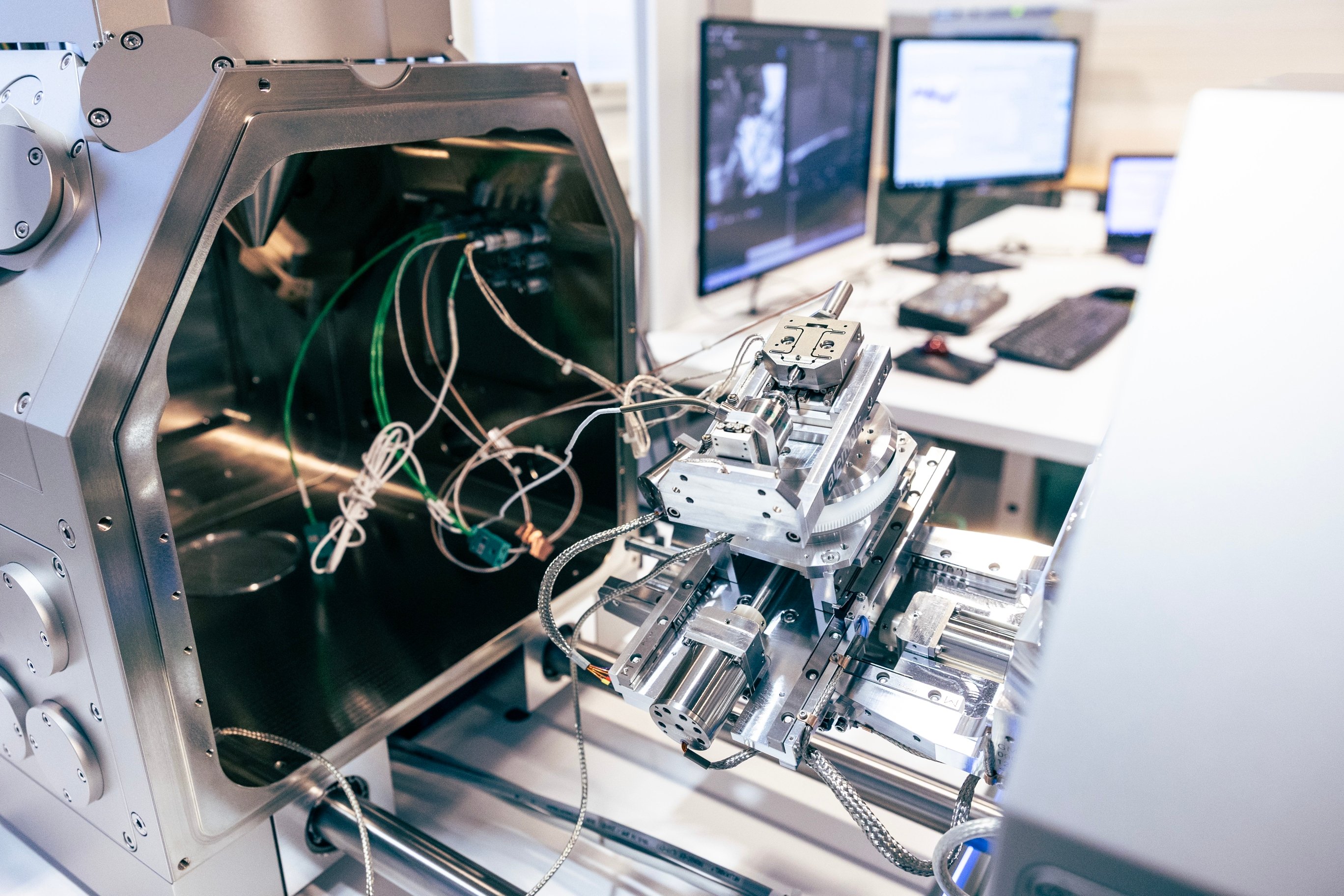 Alemnis in situ nanoindentation system in Tescan CLARA
These capabilities have been extensively utilized by the Micromechanics and Nanostructures Research Group led by Assistant Professor Gaurav Mohanty. The Tescan CLARA offers exceptional flexibility thanks to its modular design, large chamber, and multiple accessory ports. The system's capabilities will be further expanded soon with the addition of a tensile and compression testing stage, enabling even more advanced in situ mechanical characterization experiments.
In my own work, I have particularly enjoyed the high-resolution in-lens detectors, which enable excellent backscattered electron (BSE) imaging at low accelerating voltages. The LE-BSE detector has also proven to be extremely valuable. For example, we have successfully applied it in Electron Channeling Contrast Imaging (ECCI), a technique that allows the observation of crystallographic defects and deformation structures.
Looking ahead, we hope to see the versatile Tescan CLARA SEM and its growing suite of complementary characterization and testing tools serving an increasing number of collaborative research projects. The instrument forms an important part of the Operando Research Infrastructure for Energy Materials and Systems (OperaRI), which provides advanced in situ and operando characterization techniques to support scientific breakthroughs in hydrogen and other green technologies.
OperaRI is a joint research infrastructure established by the University of Oulu, VTT Technical Research Center of Finland, and Tampere University. Together, the partners have created a unique national platform that combines complementary characterization capabilities to accelerate the development of new materials, technologies, and processes for the green transition and hydrogen economy. By integrating these resources through a shared digital platform, OperaRI strengthens Finland's research ecosystem and supports innovation of national importance. The infrastructure is included in the Finnish Research Infrastructure Roadmap (FIRI) maintained by the Research Council of Finland."
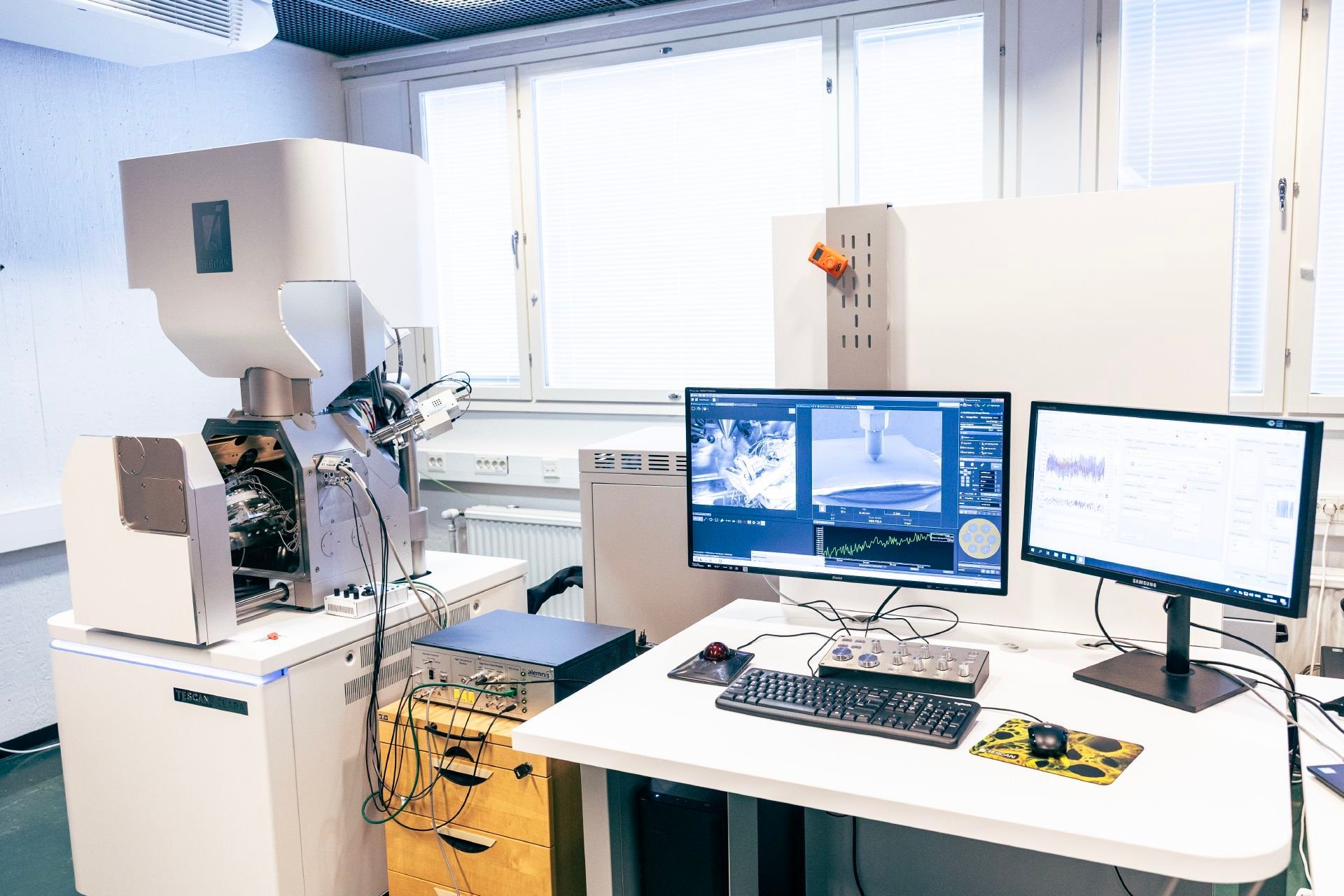 Tescan CLARA and Alemnis in situ nanoindentation system
Q: Were there any unexpected challenges or learning curves when bringing the new SEM into your lab, and what did you learn from that process?
"Over the course of my career, I have worked with numerous scanning electron microscopes from different manufacturers. Although the fundamental principles remain the same, I am still fascinated by how much the design philosophy, user interface, and overall operating experience can differ from one instrument to another. Each system has its own strengths and quirks, and becoming an expert with a new microscope always involves a learning process.
On the other hand, there are a few features from older systems that I occasionally miss. For example, a dedicated joystick for controlling the working distance. Such details may seem minor, but they can significantly influence the daily user experience, particularly for researchers who control mechanical testing systems inside the microscope."
Where Academic Research Meets Industry Collaboration
For all the precision of the instruments, the work rarely happens in isolation. Day to day, Dr. Valtonen sits where academic curiosity meets the practical questions industry brings to the lab, and it is that meeting point, more than any single technique, that she finds most rewarding.
Q: You work at the intersection of academic research and industry's practical needs. What do you find most rewarding about that collaborative role?
"What I find most rewarding is the opportunity to collaborate with researchers and industry across a wide range of disciplines and applications. Advanced characterization techniques, particularly electron microscopy, provide a unique window into the structure and behavior of materials. Whether investigating wear mechanisms, analyzing failures, or supporting the development of new materials, I am motivated by the possibility of uncovering insights that help solve real-world engineering challenges."
The Future of Material Science Research and Advanced Microscopy
If the past three decades have transformed what a microscope can reveal, the coming years promise even more. Dr. Valtonen looks ahead to a future where seeing deeper into a material is only the starting point, and where those observations increasingly guide the design of the materials still to come.
Q: Looking 5 to 10 years ahead, how do you see advanced microscopy and related technologies shaping the future of wear research and materials science?
"With advanced characterization techniques, it is possible to get detailed information for the material models that are used in multi-scale modeling. Thus, the advanced microscopy techniques open new possibilities for understanding material behavior, bridging the gap between microstructure and performance, and supporting the development of next-generation materials for demanding industrial and energy-related applications."
Key Takeaways
Dr. Kati Valtonen's work shows how advanced microscopy turns complex material behavior into practical insight. By combining wear research, in situ testing, EBSD, nanoindentation, and low-voltage high-resolution SEM imaging, she and her colleagues are building clearer links between microstructure, mechanical performance, and real-world durability. And as instruments like the Tescan CLARA join shared research infrastructures such as OperaRI, they let researchers observe wear with greater confidence and strengthen the academic and industrial collaboration that drives new materials forward.
Written by Sepideh Koubjari, Ph.D.
Content Marketing Specialist, Tescan
Explore Related Resources
Tescan CLARA™
Ultra-high-resolution SEM for advanced materials analysis.

Submit Your Sample for Advanced Contrast SEM Analysis
Improve sample analysis with advanced SEM contrast.