Reveal Subsurface Structures with Confidence
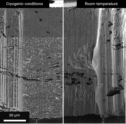
Obtain deep, clean cross-sections of electrodes and interfaces using Xe Plasma FIB with Rocking Stage™ and True X-Sectioning for artifact-free milling.

Deliver 2D and 3D insight into the internal structure and composition of battery materials with Tescan AMBER X™ 2, a high-throughput, ultra-high-resolution plasma FIB-SEM. Accelerate advanced battery research, quality assurance, and failure analysis with comprehensive multimodal characterization of both conventional and next-generation materials, ranging from the millimeter scale to the nanoscale.
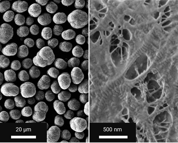
.webp?width=1279&height=1272&name=1_Surface%20morphology%20of%20cycled%20graphite%20anode%20observed%20by%20SEM%20(2).webp)
Tescan Amber X™ 2 and ToF-SIMS analysis of the SEI formation reveals how cycling protocols impact capacity retention and long-term battery performance.
.png?width=1032&height=971&name=1_Surface%20examination%20of%20exfoliation%20signs%20on%20degraded%2c%20cycled%20graphite%20anode%20particles%20(2).png)
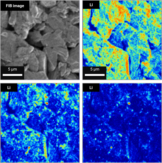
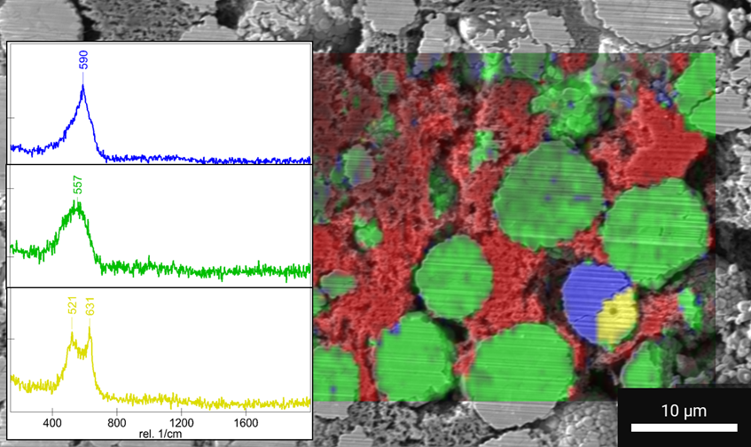
Multimodal characterization using FIB-SEM integrated with ToF-SIMS and Raman spectroscopy reveals the microstructural and chemical mechanisms behind capacity loss and internal resistance growth.

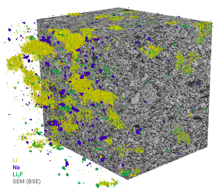
Measure electrode porosity, pore connectivity, and accessibility in 3D using high-volume FIB-SEM tomography.

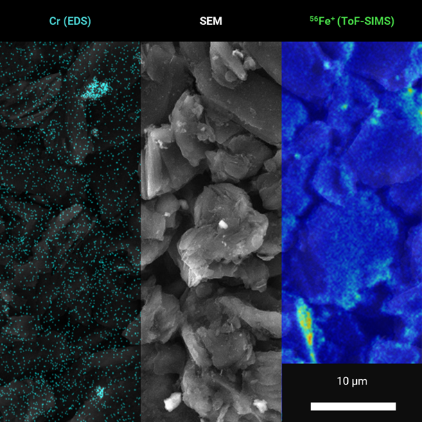
Cross-sectional imaging and elemental mapping reveal wetting behavior, lithium transport, and interface degradation in polymer-based solid-state lithium-ion cells.
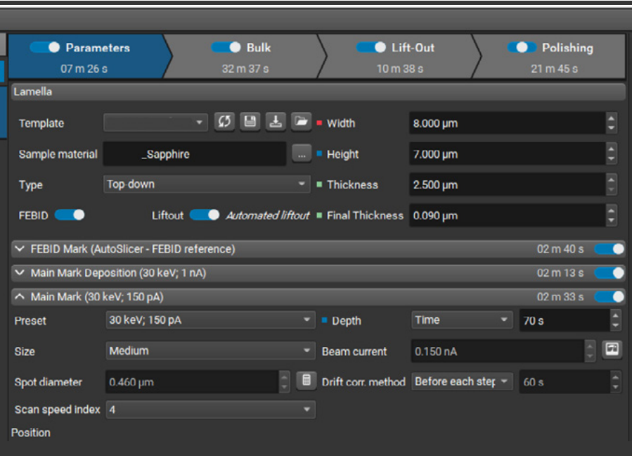
TEM AutoPrep™ and AutoPrep Pro™ streamline the full workflow—from trenching to final polishing—using AI-driven control within the Essence™ interface.
Automates milling, lift-out, and polishing for consistent, high-quality lamellae
Offers predefined or customizable workflows for electrodes, electrolytes, and solid-state samples
Handles multiple samples automatically to maximize system uptime
In battery research, AutoPrep Pro™ delivers repeatable, contamination-free TEM specimens from delicate electrodes and interfaces, enabling faster, more reliable material evaluation.