Field-Free UHR SEM Technology for Exceptional Contrast and Resolution 

BrightBeam™

BrighBeam - hero - desktop
BrighBeam - hero - mobile

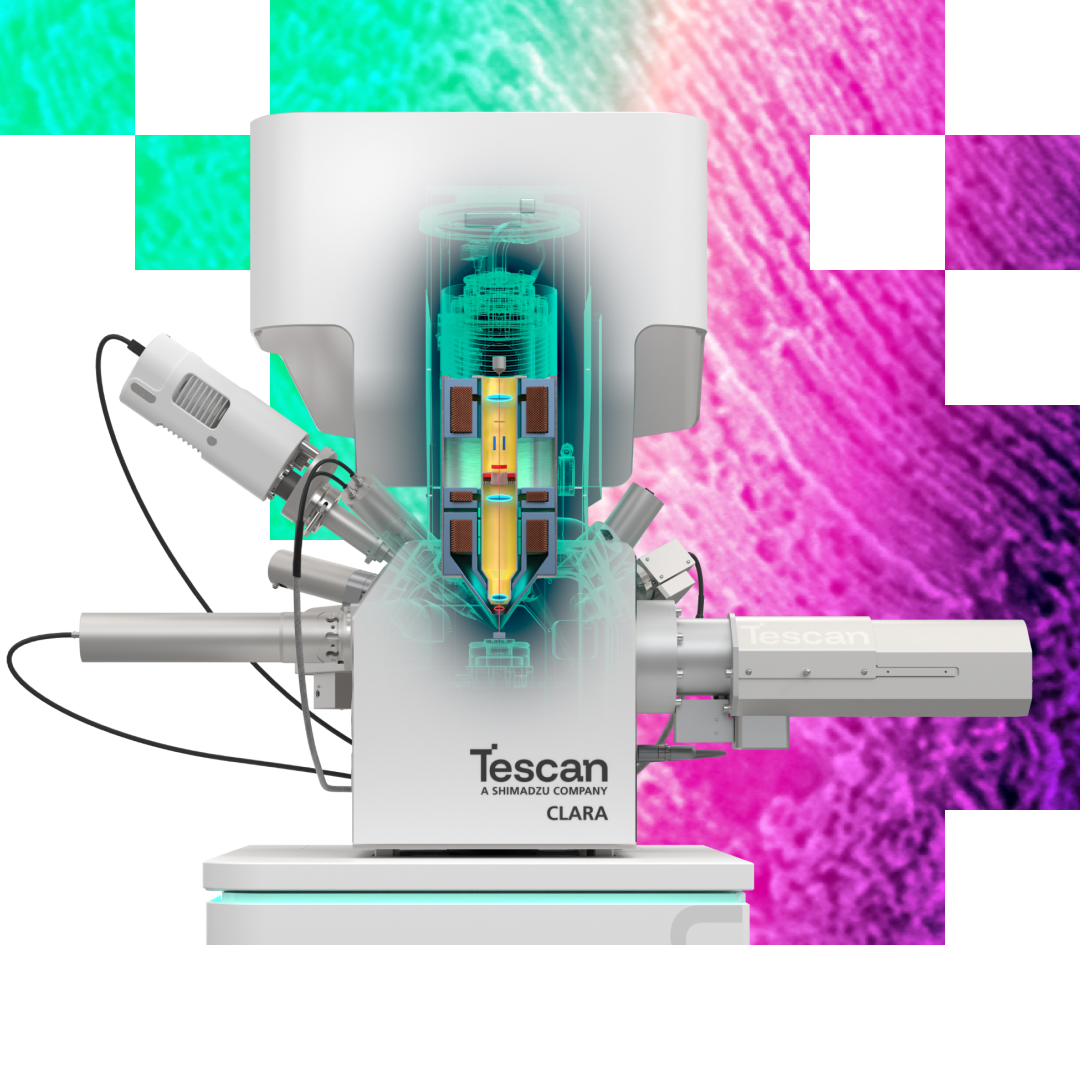
BrightBeam™ is Tescan's proprietary ultra-high-resolution electron column technology used in systems such as Tescan CLARA™, Tescan MIRA XR™, and Tescan AMBER™ 2. It combines a field-free electrostatic–magnetic objective lens, an in-column potential tube, advanced in-column electron detection, and In-Flight Beam Tracing® technology to deliver exceptional imaging performance at low landing energies. BrightBeam™ enables ultra-high-resolution field-free imaging, advanced contrast methods, and intuitive operation across a wide range of materials.

  • In-column potential tube  

  • Field-free electrostatic–magnetic objective lens
  • Ultra-high-resolution imaging at low landing energies
  • Axial and angular secondary and backscattered electron detection 
  • Energy-filtered backscattered electron imaging*
  • Selective signal filtering by electron energy and take-off angle*   
  • In-Flight Beam Tracing®  automated beam optimization
  • Wide Field Optics®  for intuitive sample navigation

Why BrightBeam™

Modern materials characterization requires more than resolution alone. Researchers need to image sensitive samples, reveal nanoscale surface details, and distinguish material differences without compromising image quality.

BrightBeam™ addresses these challenges through a unique combination of field-free electron optics, selective signal detection, and intelligent beam optimization, helping users extract more information from every scan.

Key Benefits

Ultra-High Resolution at Low Voltages 

BrightBeam™ delivers ultra-high-resolution imaging at low landing energies, enabling detailed observation of beam-sensitive, non-conductive, magnetic, and complex materials while helping reduce charging effects and preserve surface-sensitive information.
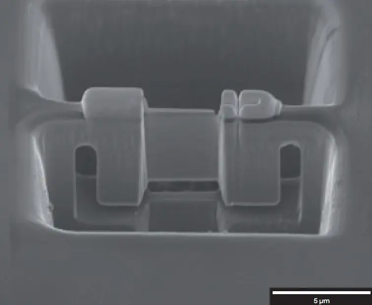
Field-Free Imaging

The BrightBeam™ column combines electrostatic and magnetic objective lens to provide field-free imaging conditions, supporting analysis of magnetic and sensitive materials while maximizing topographical information.

Exceptional Contrast Method Versatility* 

Advanced in-column detectors selectively filter electrons according to both their energy and take-off angle, enabling enhanced topographical, compositional, and materials contrast from the same region of interest.  

Simplified Operation with In-Flight Beam Tracing™ 

Integrated In-Flight Beam Tracing®  continuously models and optimizes beam conditions in real time, enabling fast setup of imaging and analytical workflows without manual column adjustments. 

Applications

BrightBeam™ is designed for advanced characterization of

Materials and metallurgy 

Battery materials

Nanomaterials

Beam-sensitive samples 

Magnetic materials 

Semiconductor research  

Failure analysis

Academic and industrial R&D 

* Feature availability depends on the instrument model.
Unlocked content


Tescan Orage 2 APPLICATION EXAMPLES


[application examples in few words]


Unlock Tescan insight

leave a contact to access

Get the most out of Tescan

This is more than information; it's an advantage. We've compiled our technical whitepapers, detailed product flyers, and on-demand webinars to provide you with the knowledge that makes a real difference. Sign up now to access the insights you need to make an impact.

4D-STEM detector

Technical specification

Detector type

Solid state, hybrid pixel detector

Technology

Timepix 3 chip by AdvaScope, Peltier cooled

Chip parameters

256 × 256 pixel matrix; pixel size 55 µm × 55 µm

Detection limit

5 keV

Readout throughput

High throughput, 40 million hits·s¹·cm² 

Acquisition mode

 Data-driven 

Control

Fully integrated into Tescan EssenceTM, motorised

Image acquisition

Live imaging: up to 2 µs/pixel

2D imaging: Diffraction patterns and/or Kikuchi lines, Bright-Field and Dark-field imaging based on user-selectable virtual apertures

4D-STEM: data cubes

Protection

Integrated shutter and interlocks

Detector type

Solid state, hybrid pixel detector

Technology

Timepix 3 chip by AdvaScope, Peltier cooled

Chip parameters

256 × 256 pixel matrix; pixel size 55 µm × 55 µm

Detection limit

5 keV

Readout throughput

High throughput, 40 million hits·s¹·cm² 

Acquisition mode

 Data-driven 

Control

Fully integrated into Tescan EssenceTM, motorised

Image acquisition

Live imaging: up to 2 µs/pixel

2D imaging: Diffraction patterns and/or Kikuchi lines, Bright-Field and Dark-field imaging based on user-selectable virtual apertures

4D-STEM: data cubes

Protection

Integrated shutter and interlocks

4D_STEM_isolated_priruba_left_05-1024px

GET IN Touch

with specialist

map

Where you can find us:

Tescan Brno
Libušina třída 21
623 00 Brno
Czech Republic


130405923 us US 37.09024 -95.712891 25.3575 29.349345 20.67957527 42.082797 39.91384763 -33.693421 13.93320106 3.039986586 31.997988 38.050985 47.579533 48.1485965 58.375799 54.663142 19.195447 56.975106 47.916997 50.493053 45.868592 10.79556993 44.35660598 43.2371604 55.536415 14.557577179752773 32.100937 -6.116829 -6.212299277967318 33.600194 -12.08688 23.7104 -33.471062 31.998740087 -23.69149395 43.462349 51.529848 49.1893523 49.197486 25.072375 31.075811 1.299027 40.676979 52.30150662 51.013813 35.684121 37.566531 52.246622 40.581349 39.911632 -26.1811371 41.818215 33.429928

No distributors found.