Effortless Imaging and Analysis
Easily switch between imaging and EDS analysis within a single live window using Essence™ EDS. This integration simplifies workflows and cuts down the time spent switching between tools.

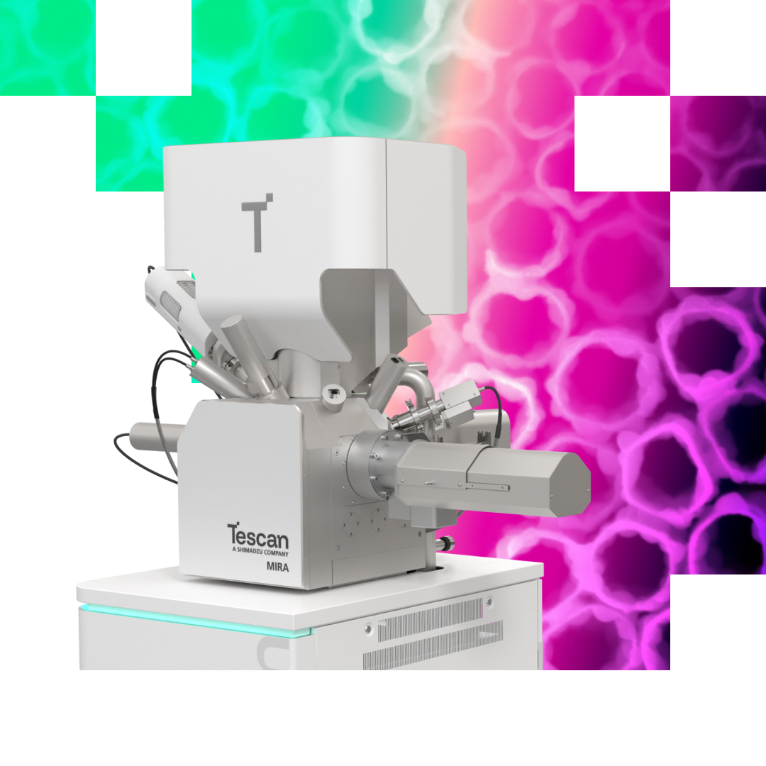
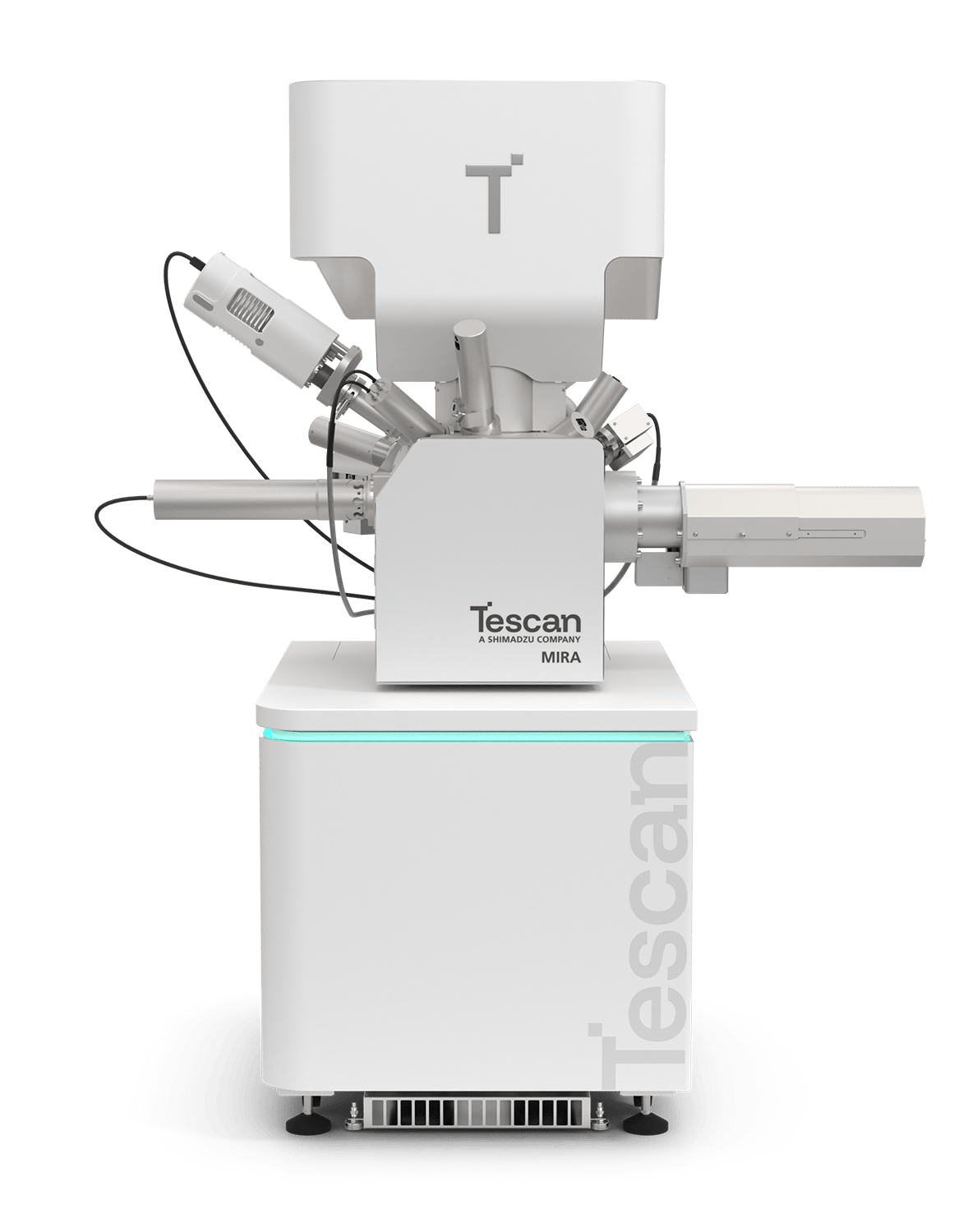
Tescan MIRA™ scanning electron microscope pairs a FEG (Field Emission Gun) Schottky source with integrated SEM imaging and live elemental analysis in a single Essence™ software window, simplifying the acquisition of morphological and compositional data.
Tescan MIRA™ is a practical analytical tool for quality control, failure analysis, and research workflows, offering fast navigation, flexible vacuum modes, and efficient operation across diverse materials.

Tescan MIRA™ helps materials laboratories connect surface morphology with elemental composition across metals, ceramics, polymers, and composites. Combining field-emission SEM imaging with integrated analytical tools and straightforward operation, it supports everyday characterization needs in research and industrial laboratories within one practical workflow.
Reveal surface features and material differences with complementary SE and BSE imaging, helping build a fuller understanding of each sample.
Connect images with elemental composition using integrated Essence™ EDS, keeping morphological and chemical information together in one software environment.
Locate representative areas quickly with Wide Field Optics™, moving directly from a sample overview to the features that need investigation.
Simplify transitions between imaging and analysis with automated beam setup, reducing manual adjustments as characterization tasks and sample requirements change.
Support shared laboratory workflows with configurable Essence™ layouts and presets, while the 3D Collision Model helps users move samples confidently and avoid collisions.
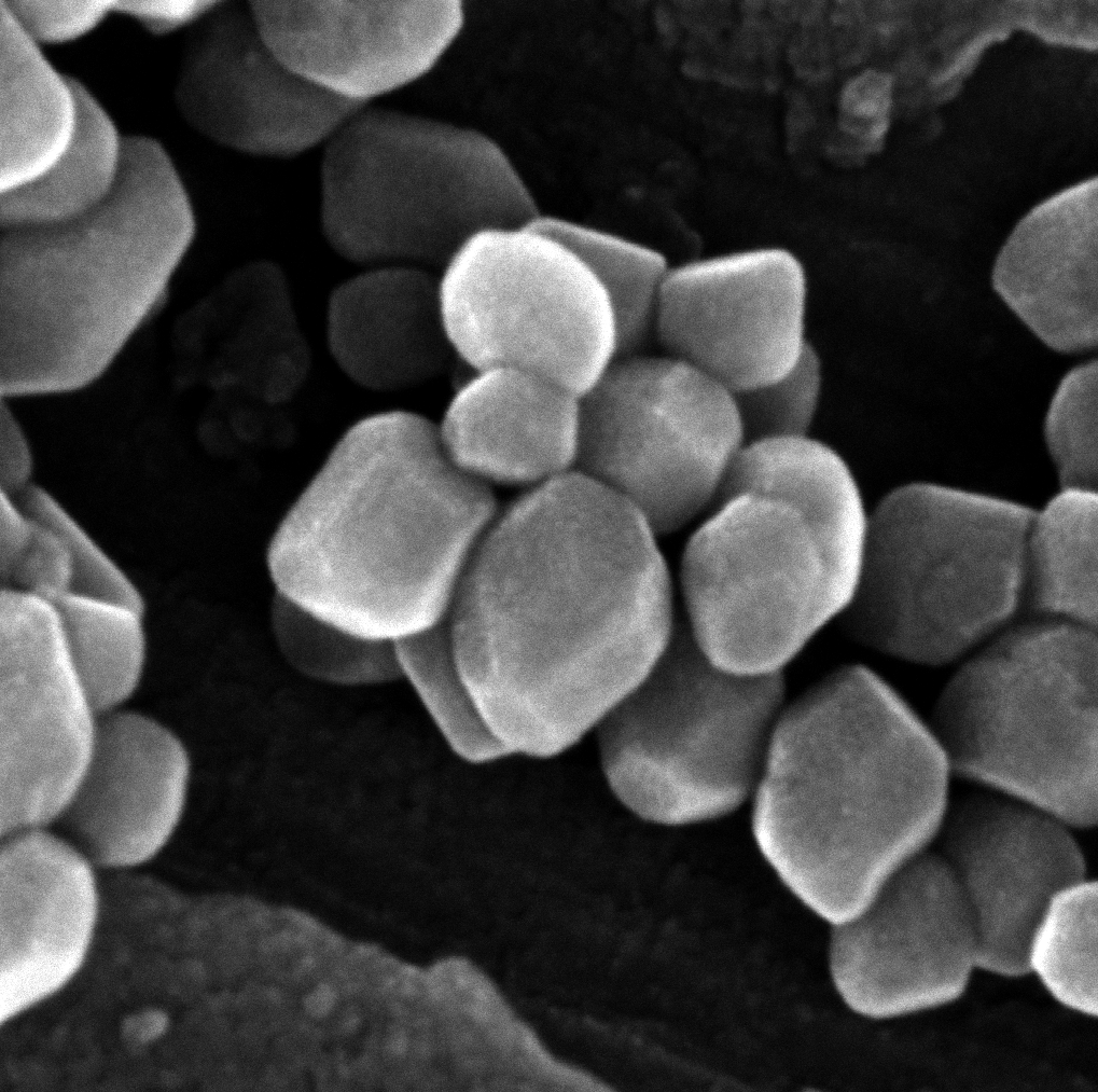
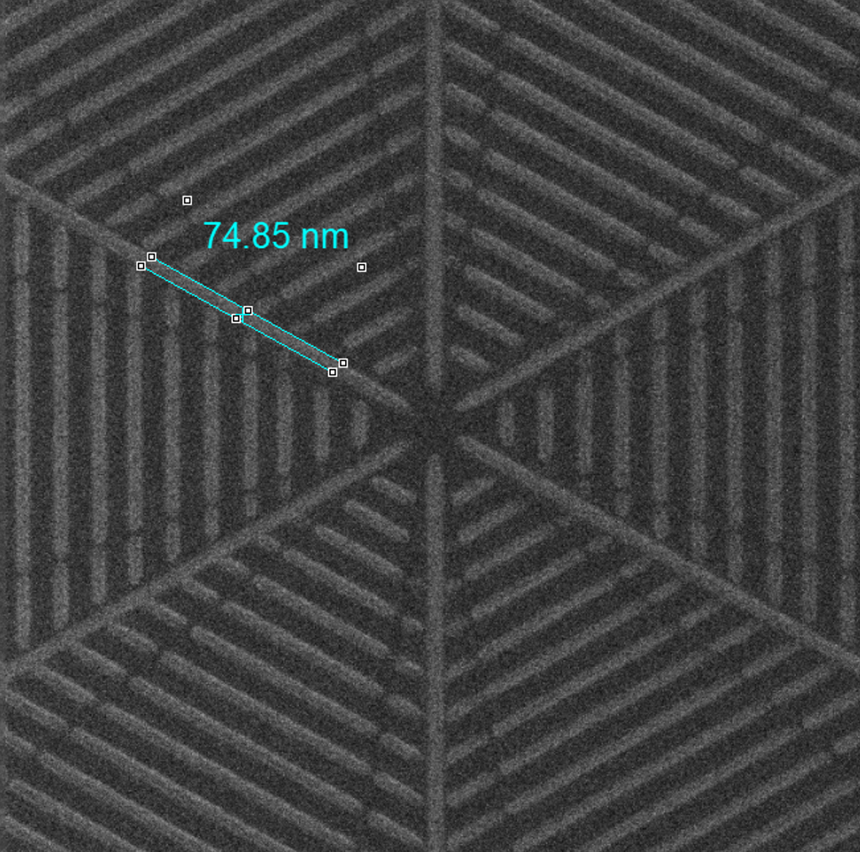
Tescan MIRA™ equipped with the Nanoprototyping Toolbox combines proven high-performance SEM imaging with integrated nanofabrication capabilities — giving researchers and R&D engineers a dependable platform to move from concept to functional prototype.
Design and fabricate novel 2D/3D structures directly in the SEM — from plasmonic arrays to quantum device layouts
Achieve precise nanoscale patterning for demanding lithography and prototyping applications on a time-tested, high-performance platform
Fabricate or etch structures directly — no resists, no extra steps — using integrated gas injection for in-situ material deposition
Analyse and iterate prototypes in-situ, reducing turnaround times from weeks to hours
Automate even complex prototyping routines end-to-end with Python API and block-based automation — no programming expertise required
Tescan MIRA™ extends nanoscale research capabilities with a fully integrated environment for fabrication and analysis — one microscope, one software, total control. Its proven reliability and high-resolution imaging make it a trusted workhorse for researchers and engineers who need consistent performance across diverse nanoprototyping workflows. Whether you're developing nanostructured sensors, refining lithography processes, or scaling up prototype iterations, MIRA™ delivers the precision and dependability your research demands.
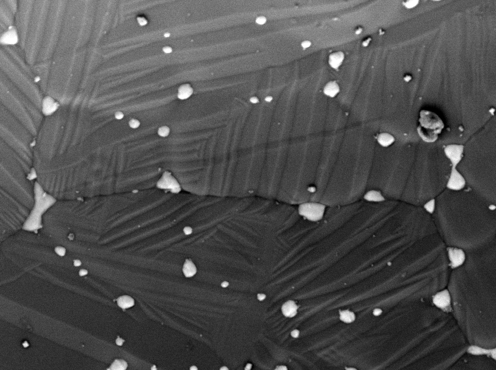
Tescan MIRA™ helps metallurgy laboratories connect microstructural observations with elemental composition when examining metals and alloys. Combining detailed SEM imaging with accessible analytical workflows, it supports investigations of material quality and performance, from polished sections to fractured components, within a dependable platform for routine laboratory use.
Examine polished sections with BSE imaging to distinguish material contrast and locate features for closer investigation, supporting comparisons between samples and processing conditions.
Investigate inclusions and local compositional differences with integrated Essence™ EDS, connecting elemental information to specific features observed in the metal microstructure.
Explore fracture surfaces with SE imaging and extended depth of focus, keeping uneven features visible while examining the morphology of damaged components.
Navigate from an overview to individual features with Wide Field Optics™, helping maintain sample context when examining cross-sections, fractures, or tilted analytical samples.
Extend characterization with optional EBSD, complementing imaging and elemental analysis when a laboratory needs additional crystallographic information from its metal samples.
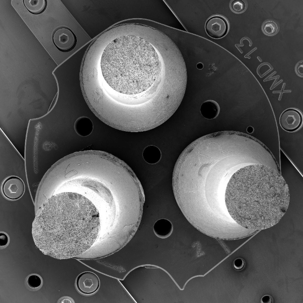
Tescan MIRA™ supports quality control and failure analysis by bringing detailed imaging and elemental analysis into a straightforward inspection workflow. From routine checks to investigations of unexpected material behavior, it helps industrial laboratories examine defects, compare material features, and document evidence for informed decisions.
Inspect surfaces, polished cross-sections, and fractures with SE and BSE imaging to reveal defects, inclusions, and differences within components and materials.
Investigate particles and suspected contamination with integrated Essence™ EDS, linking elemental findings directly to the feature being examined in the SEM.
Find areas of interest quickly with Wide Field Optics™, then zoom into individual features without losing the wider context of the sample.
Streamline recurring inspection tasks with configurable Essence™ presets, helping users return to established imaging conditions across routine laboratory workflows and investigations.
Keep SEM images and corresponding EDS results together in an stored dataset, making inspection evidence easier to retrieve, review, and complement.

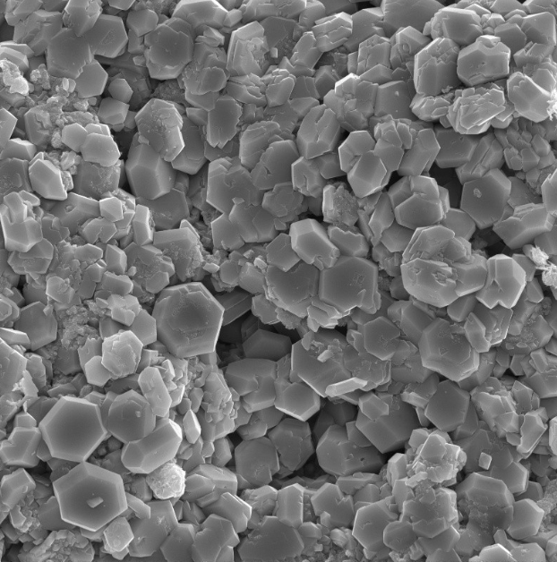
Tescan MIRA™ supports advanced geoscience characterization with a field-emission SEM platform designed for high-resolution imaging and detailed microanalysis.
Reveal fine mineral textures, grain boundaries, and microstructural features using high-resolution secondary and backscattered electron imaging.
Use integrated Essence™ EDS to identify mineral phases, investigate compositional variations, and correlate elemental information with mineral textures.
Extend geological characterization with optional cathodoluminescence, EBSD, WDS, and Raman techniques for more comprehensive mineral and microstructural analysis.
Consider the TIMA™ option to add automated mineralogy capabilities.
High Resolution SEM Imaging and Microanalysis for Diverse Material Analysis
Tescan MIRA enables detailed sub-micron analysis of metals, ceramics, polymers, and composites. Its stable FE source, flexible detectors, and unified SEM–EDS workflow support consistent, application-ready data across diverse research needs.
Fast, dependable SEM workflows for routine inspection tasks
Sub-micron inspection for device, interconnect, and wafer-level evaluation
MIRA helps semiconductor and electronics teams with examining device faults, structural irregularities, and various inspection tasks. Featuring a stable FEG source, navigation, and integrated analytical tools, it reveals fine geometries and subtle features. This supports reliable assessments throughout device workflows. It simplifies acquiring morphological and elemental data, making it an efficient solution for quality control, failure analysis, and research in microelectronics.
Unified Control for Imaging and Analysis
Tescan Essence™ offers a modular interface for MIRA™, allowing users to manage imaging, navigation, and microanalysis within a single customizable layout. This adjustable design promotes efficient, consistent workflows for both routine and advanced SEM tasks.