About the event
SPIE Photonics West is a leading international conference and exhibition for optics and photonics technologies. Organized by SPIE, the event brings together researchers, engineers, and industry professionals working in biomedical optics, industrial lasers, optoelectronics, microfabrication, quantum technologies, and advanced imaging.
Tescan at Photonics West
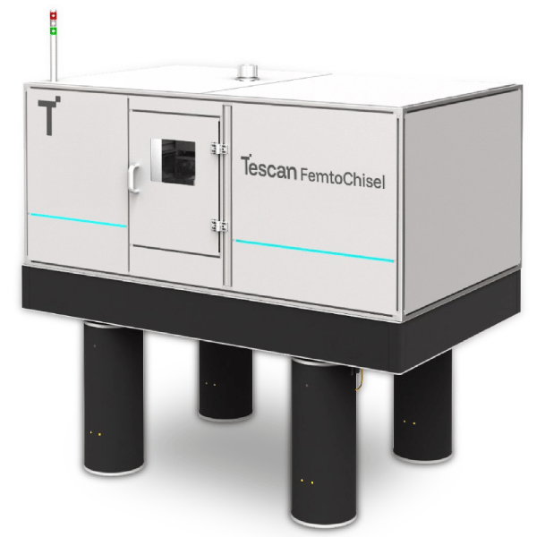
Visit Tescan at Booth 2162 to explore FemtoChisel™, our femtosecond laser processing technology for precision material removal, microfabrication, and sample preparation.
Learn how ultrafast laser processing, AI-assisted optimization, and correlative microscopy can support complex workflows involving optical materials, semiconductor devices, and biological samples.
Tescan will also contribute four scientific presentations exploring AI-enabled femtosecond laser applications, from precision machining of sapphire and fused silica to semiconductor analysis, hybrid manufacturing, and biological sample preparation.
Featured technology: Tescan FemtoChisel™
Precision laser processing for complex materials and applications
Tescan FemtoChisel™ uses femtosecond laser technology for precise material modification and sample preparation. Its capabilities support localized material removal, drilling, cross-sectioning, surface structuring, and microfabrication.
At Photonics West, discover applications including:
-
Optical materials: Precision machining, microstructuring, and welding of sapphire and fused silica.
-
Semiconductors: Targeted access, controlled delayering, and cross-sectioning for failure analysis and process verification.
-
Advanced manufacturing: Laser-assisted material removal integrated with imaging and inspection workflows.
-
Life sciences: Site-specific preparation of resin-embedded biological samples for multimodal microscopy.
Scientific presentations
Join Dr. Pouya Tavousi, Head of AI and Advanced Solutions at Tescan, for four presentations examining AI-assisted femtosecond laser processing and correlative workflows.
January 31, 2027 | 4:30–4:50 PM PST
AI-optimized femtosecond-laser preparation of resin-embedded biological samples for multimodal microscopy
Explore an integrated femtosecond laser workflow for preparing resin-embedded biological tissue for optical, X-ray, and electron microscopy. The presentation covers automated tool-path generation, in-situ optical imaging, and AI-assisted parameter optimization to improve preparation accuracy and reproducibility.
February 1, 2027 | 2:40–3:00 PM PST
AI-enabled correlative femtosecond-laser platform for semiconductor analysis, process verification, and device fabrication
Learn how AI-assisted femtosecond laser processing integrates X-ray CT, optical microscopy, and SEM for targeted semiconductor analysis. The presentation examines defect localization, controlled delayering, precision machining, and automated process planning within a shared coordinate framework.
February 2, 2027 | 4:40–5:00 PM PST
AI-planned hybrid additive-subtractive manufacturing in a universal correlative coordinate framework
Discover a hybrid manufacturing approach connecting additive fabrication, femtosecond laser material removal, and multimodal characterization. The presentation explores how AI-assisted planning and shared coordinate systems enable targeted machining, inspection, and corrective processing.
February 4, 2027 | 9:30–9:50 AM PST
AI-optimized femtosecond-laser processing of sapphire and fused silica for holes, surface features, and precision welding
Explore AI-assisted laser machining and welding of challenging optical materials. The presentation covers precision drilling, surface structuring, and localized welding, with process optimization focused on feature quality, repeatability, and minimizing material damage.
Who should attend?
This is ideal for optics and photonics researchers, laser processing and microfabrication specialists, semiconductor failure analysis and process engineers, materials scientists, advanced manufacturing researchers, biomedical imaging and microscopy specialists, and academic and industrial researchers exploring AI-assisted manufacturing.
Registration
Meet Tescan at SPIE Photonics West 2027
Visit Booth 2162 to speak with our specialists about femtosecond laser processing, AI-assisted workflows, and applications for your research or manufacturing needs.