Deliver Deep, Artifact-Free Cross Sections
Achieve clean, reliable results on complex IC packages using Rocking Stage™ and TRUE X-sectioning.
WEBINAR | Tailored Cryo-EM and Correlative Workflows for Challenging Biological Projects
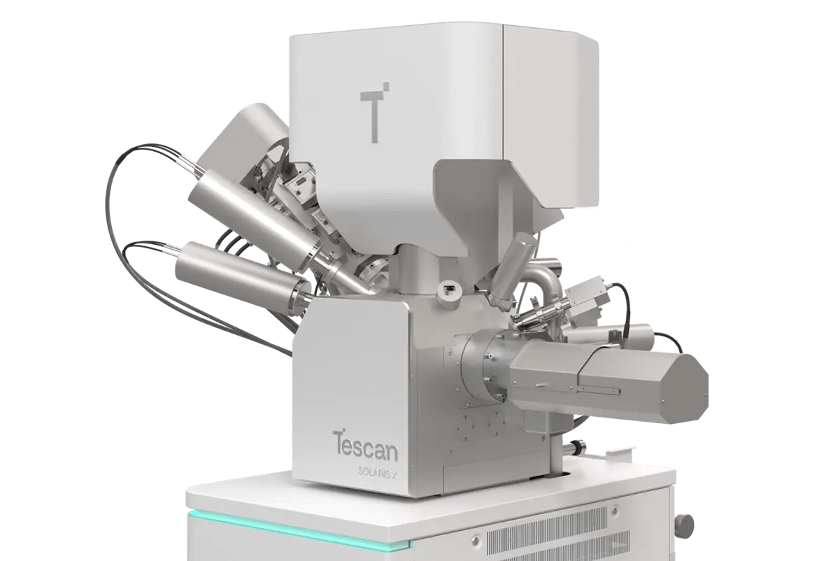
Solve package-level failure challenges with Tescan SOLARIS X™ 2 Plasma FIB-SEM. Designed for today’s complex IC packaging, SOLARIS X™ 2 combines the Mistral™ Xe Plasma FIB column with Rocking Stage™, TRUE X-sectioning, and the Triglav™ UHR SEM to deliver deep, clean cross-sections and precise end-pointing.
Deliver Deep, Artifact-Free Cross Sections
Achieve clean, reliable results on complex IC packages using Rocking Stage™ and TRUE X-sectioning.
Pinpoint Subsurface Defects with Precision
Detect cracks, voids, and delaminations using Triglav™ UHR SEM end-pointing at the FIB-SEM coincidence point.
Prepare Ga+-Free TEM Lamellae Efficiently
Protect device integrity while producing high-quality, contamination-free lamellae with the Mistral™ Xe Plasma FIB column.
Cross-Section the Toughest Materials
Section SiC, polyimide, glass, and ceramics with uniform surfaces, free of curtaining and terrace artifacts.
Boost Throughput Across Workflows
Leverage 3.3 µA Xe+ beam currents and automated column alignments for faster, more consistent sample preparation.
Maintain Clarity at Every Scale
Resolve fine package details with Triglav™ UHR SEM imaging at accelerating voltages down to 500 eV.
Achieve accurate, geometry-true cross-sections with the Hybrid Laser and Plasma FIB Workflow using CAD/GDS overlay navigation.
Perform physical failure analysis of MEMS motion sensors using Tescan SOLARIS X™ 2 with artifact-free cross-sectioning that protects bonding layers and eliminates delamination risks.
Create a reliable OLED display cross section using Tescan SOLARIS X™ 2 with precise layer control that preserves structure and avoids sample damage.
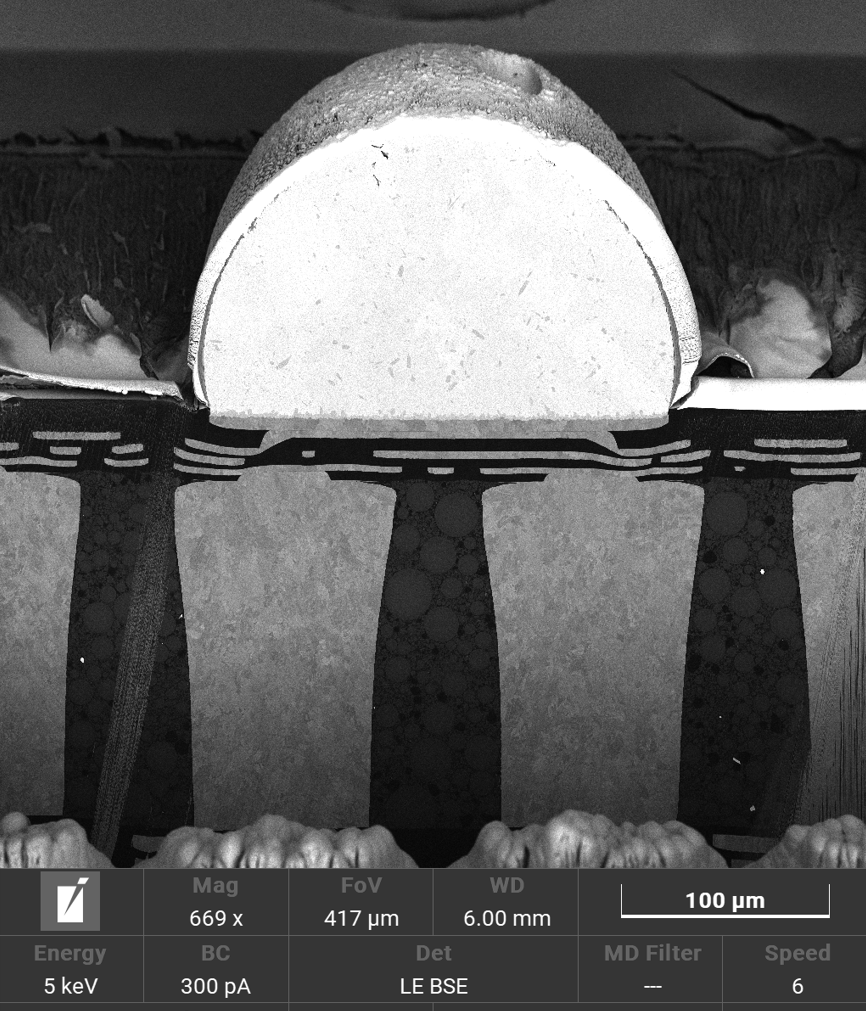
Apply Tescan SOLARIS X™ 2 with Rocking Stage™ to achieve smooth, artifact-free plasma FIB cross sections for TSVs, solder bumps, and MEMS packaging structures.
Perform TEM lamella preparation on 7nm node transistors using Tescan SOLARIS X™ 2 with in-situ delayering and thinning that maintain structural fidelity and eliminate air exposure.
Use Tescan SOLARIS X™ 2 with Mistral™ Xe plasma FIB for TEM sample preparation of SDRAM devices. Produce thin, Ga+-free lamellae that preserve interface quality and elemental contrast at the 66 nm node.
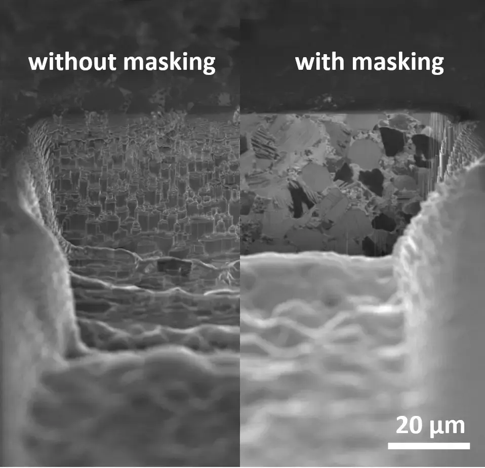
Tescan TRUE X-sectioning™ gives you clean, reliable cross sections for package-level failure analysis. Precut silicon masks combined with optimized plasma FIB milling suppress ripple artifacts that would otherwise obscure critical features. When paired with Rocking Stage™, you also eliminate curtaining, achieving smooth, uniform surfaces, even in challenging materials like SiC, polyimide, and glass.
With TRUE X-sectioning™, you get cross sections you can trust for defect detection and high-resolution imaging. It streamlines your workflows and improves the consistency of your results.
This is more than information; it's an advantage. We've compiled our technical whitepapers, detailed product flyers, and on-demand webinars to provide you with the knowledge that makes a real difference. Sign up now to access the insights you need to make an impact.
|
SOLARIS X™ 2
|
Electron column: Triglav™ UHR SEM with immersion optics |
|---|---|
|
Ion column: Mistral™ Xe Plasma FIB, 500 eV–30 keV, probe current <1 pA–3.3 µA, resolution <10 nm @ 30 keV |
|
|
Stage: Motorized 5-axis Compucentric Stage with Tescan Rocking Stage™ |
|
|
Lift-out compatibility: in situ with TEM AutoPrep™ Pro or ex situ with Tescan EXLO™ |
|
|
Optical microscope: Tescan ONCam™ Navigation Camera |
|
|
Nanomanipulator: Tescan OptiLift™ |
|
|
Grid compatibility: NCD slotted grids, EXpressLO PGrids™ (Cu, Ni); for standard and inverted TEM samples |
|
|
Detectors: In-beam SE and BSE detectors; STEM imaging at 0.5 nm resolution @ 30 keV |
|
|
Automation: Scheduled electron/ion column alignments for continuous system readiness |
|
SOLARIS X™ 2
|
|---|
|
Electron column: Triglav™ UHR SEM with immersion optics |
|
Ion column: Mistral™ Xe Plasma FIB, 500 eV–30 keV, probe current <1 pA–3.3 µA, resolution <10 nm @ 30 keV |
|
Stage: Motorized 5-axis Compucentric Stage with Tescan Rocking Stage™ |
|
Lift-out compatibility: in situ with TEM AutoPrep™ Pro or ex situ with Tescan EXLO™ |
|
Optical microscope: Tescan ONCam™ Navigation Camera |
|
Nanomanipulator: Tescan OptiLift™ |
|
Grid compatibility: NCD slotted grids, EXpressLO PGrids™ (Cu, Ni); for standard and inverted TEM samples |
|
Detectors: In-beam SE and BSE detectors; STEM imaging at 0.5 nm resolution @ 30 keV |
|
Automation: Scheduled electron/ion column alignments for continuous system readiness |
Tescan
Libušina třída 21
623 00 Brno
Czech Republic
No distributors found.