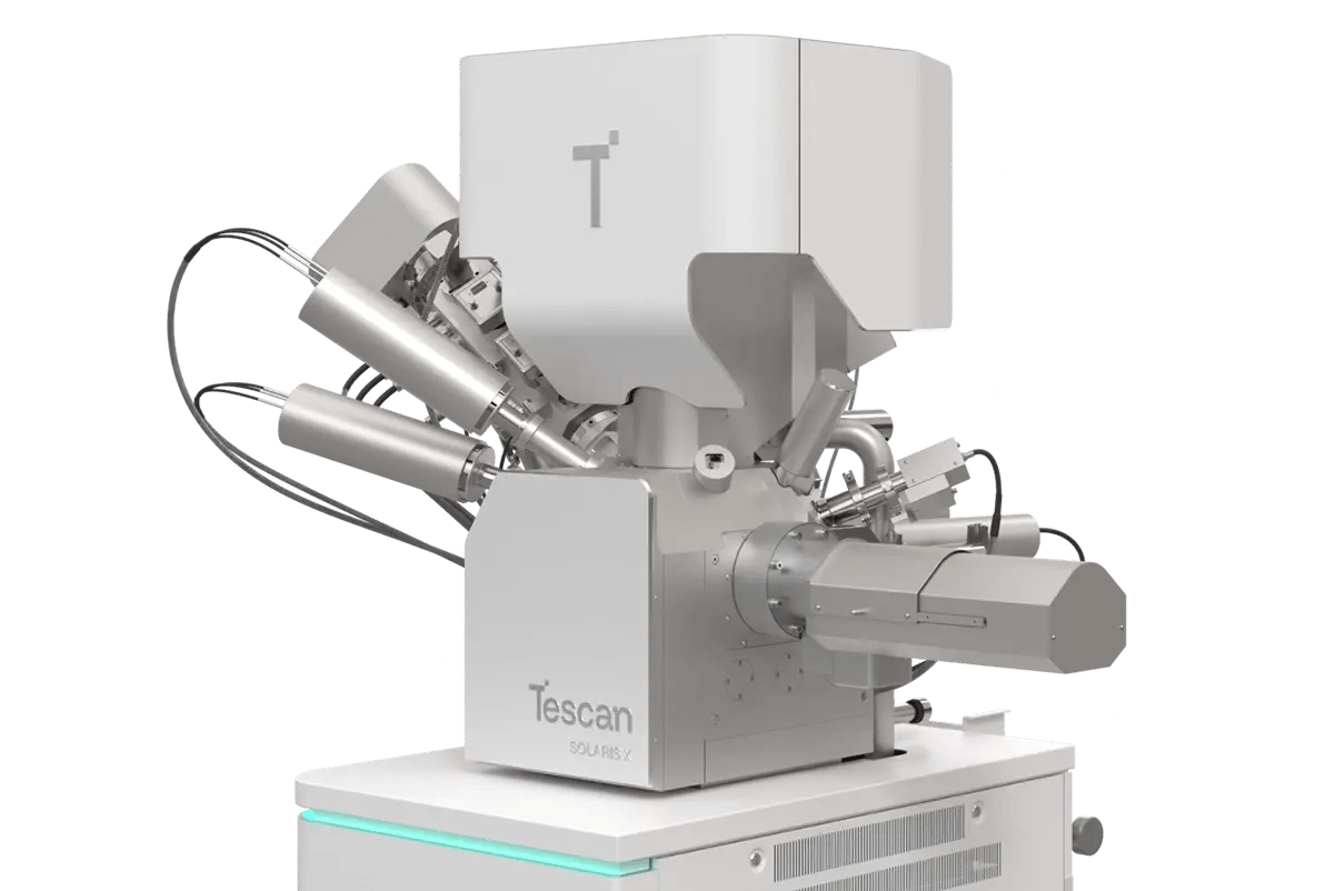
Tescan SOLARIS X™ 2 FIB-SEM
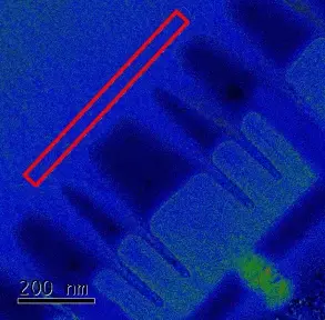
Tescan SOLARIS X™ 2 FIB-SEM delivers the precision, control, and integration required for preparing sub-20 nm TEM lamella from 7nm node devices.
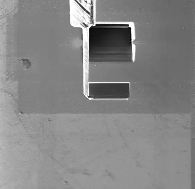
The Xe⁺ plasma-based system combines gas-assisted delayering, trenching, and thinning within a single, in-situ workflow—eliminating air exposure and reducing variability.
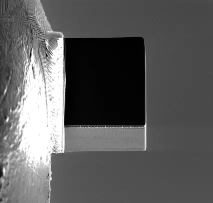
OptiLift™ nanomanipulation supports stable lamella handling, while low-keV final polishing ensures structural integrity for high-resolution imaging.
- Integrated Xe⁺ plasma FIB-SEM platform: Complete TEM preparation without transferring between systems
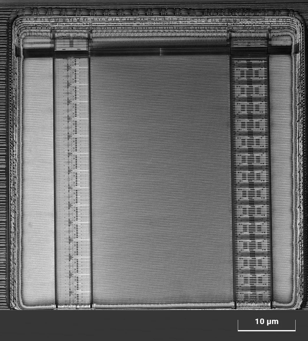
- Gas-assisted delayering: Remove layers from M10 to contact with control and repeatability
- In-situ lift-out with OptiLift™: Reduce mechanical stress and contamination during lamella transfer
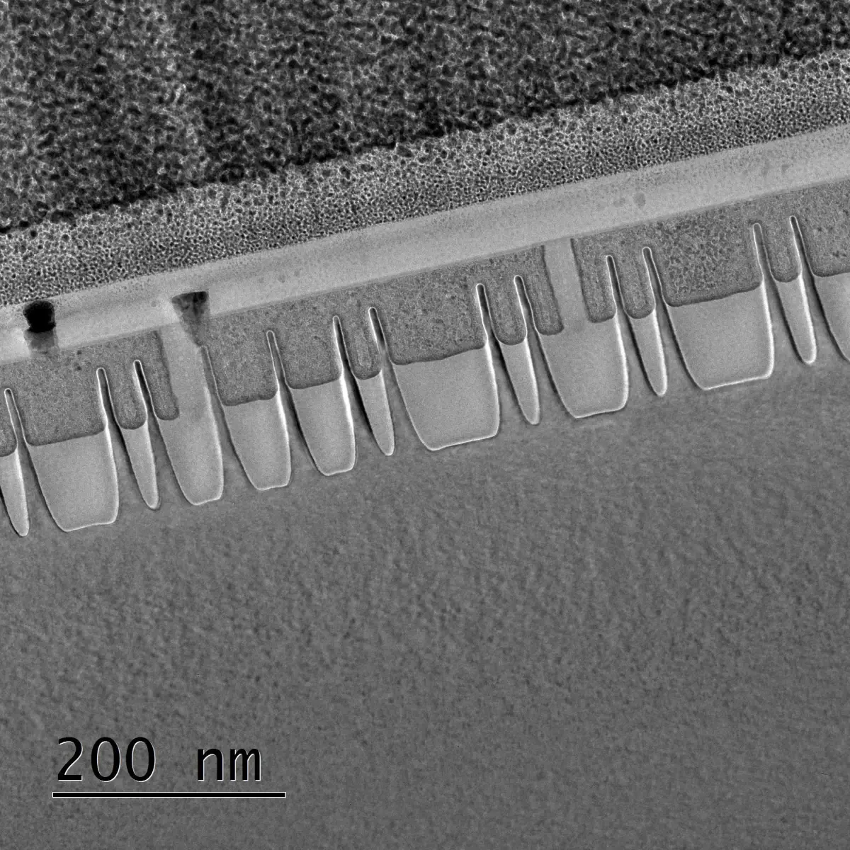
- Sub-20 nm lamella preparation: Achieve transistor-level resolution suitable for HR-TEM or STEM
- Inverted geometry and 1 keV final thinning: Minimize curtaining and preserve structural accuracy across layers