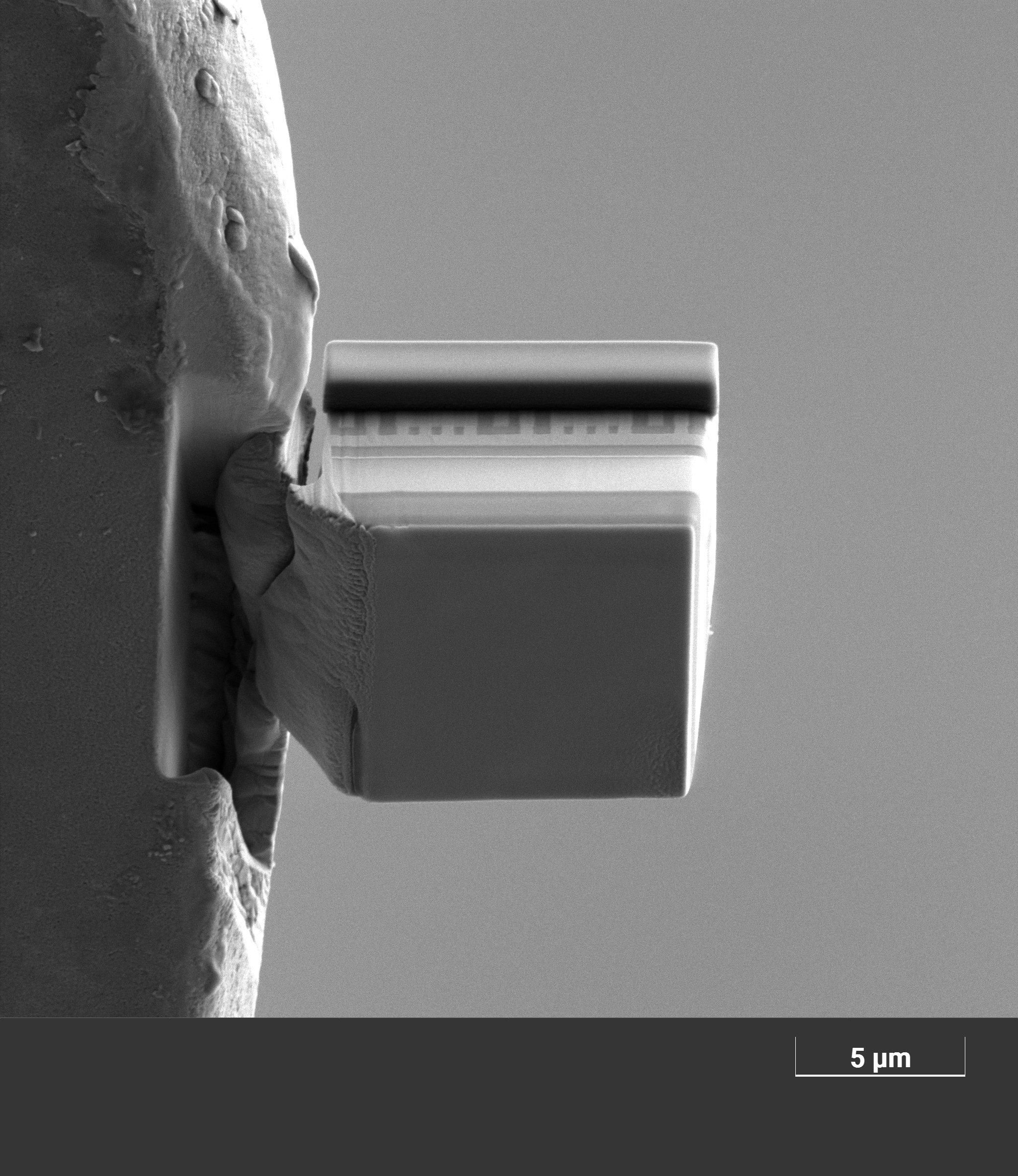
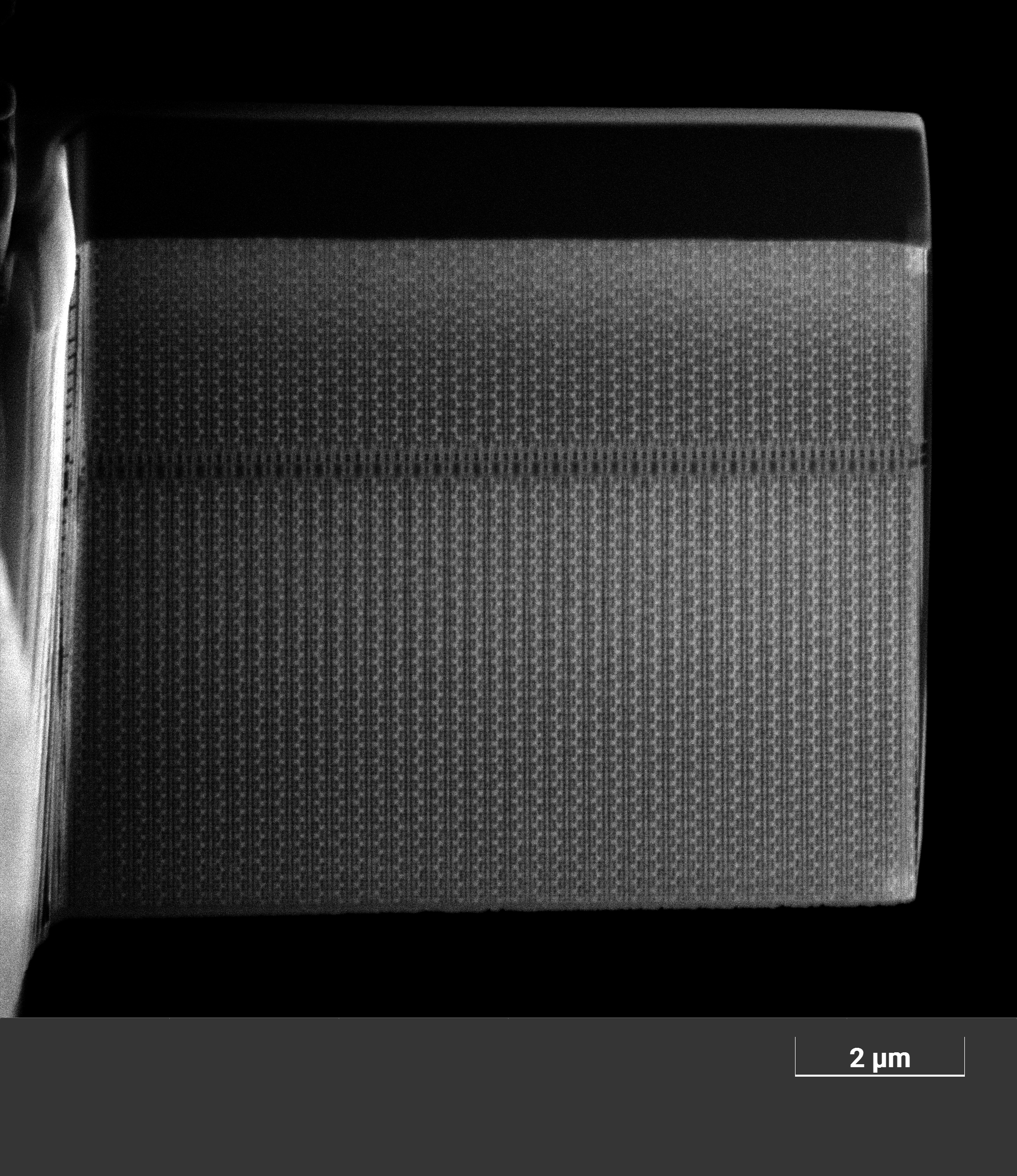
test
test video
WEBINAR | Correlated Microanalytical Workflows for Particle Analysis Using Automated Mineralogy, FIB-SEM and SIMS
Ga⁺ FIB column - Built for Semiconductor Performance
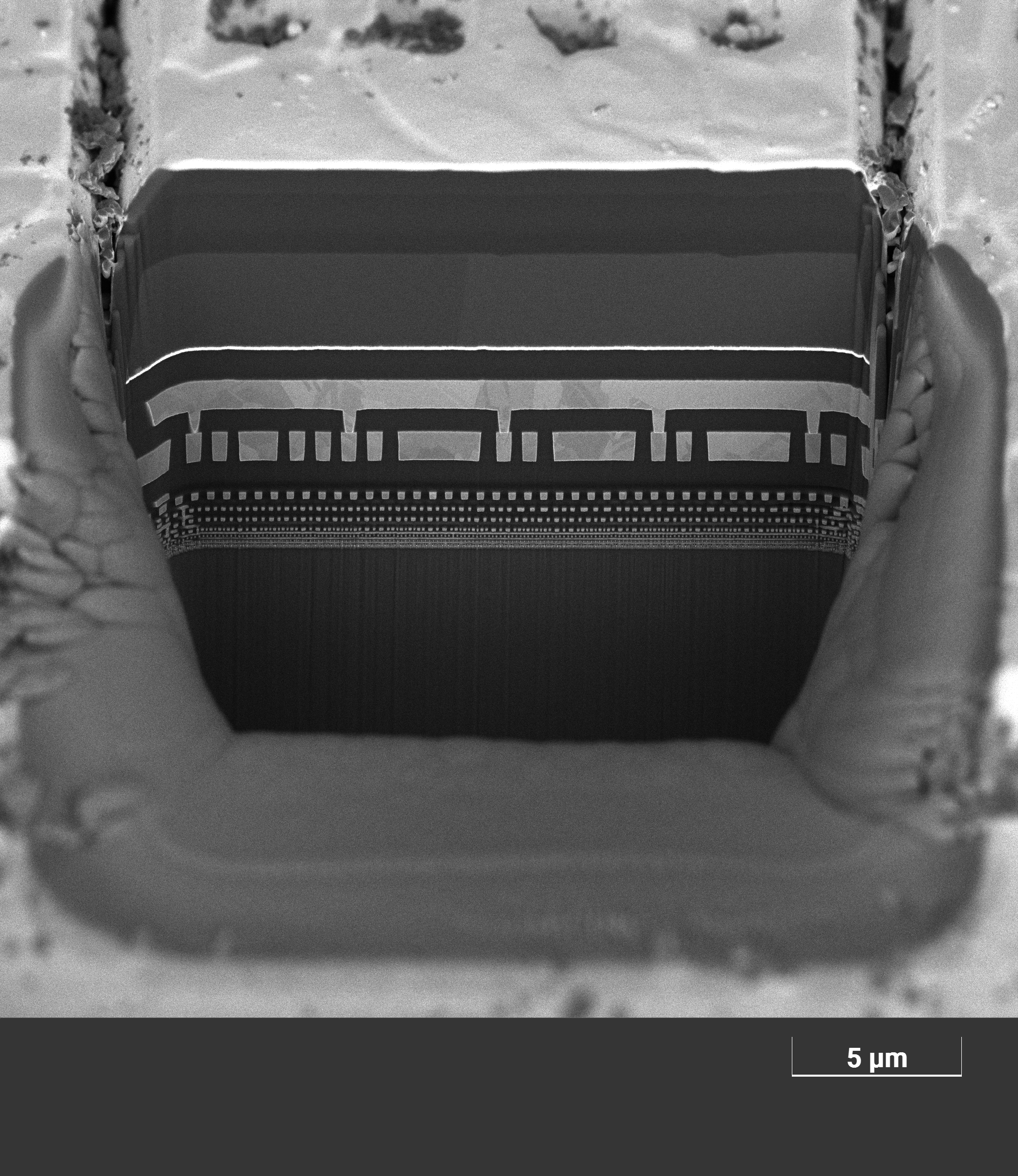
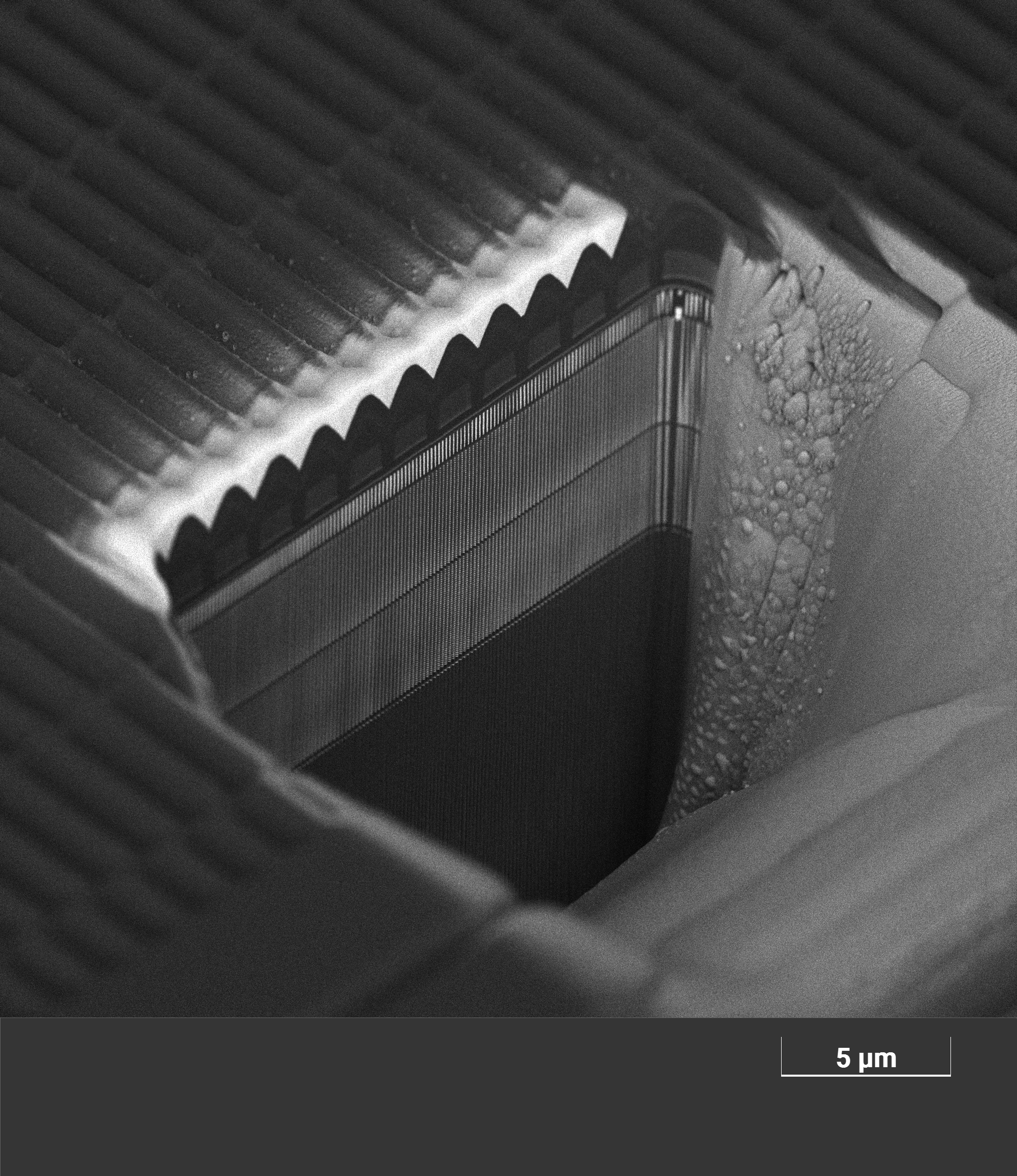
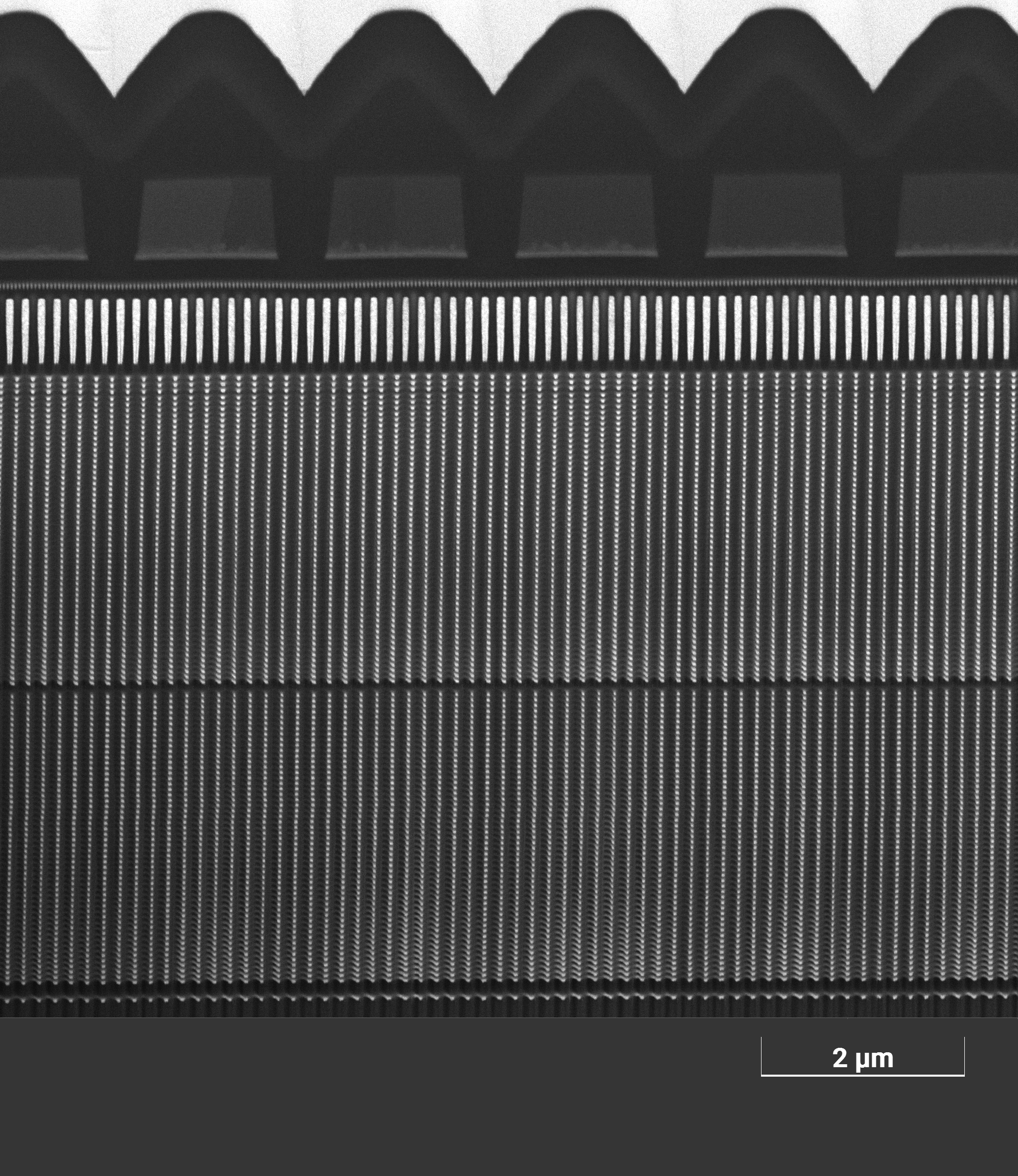
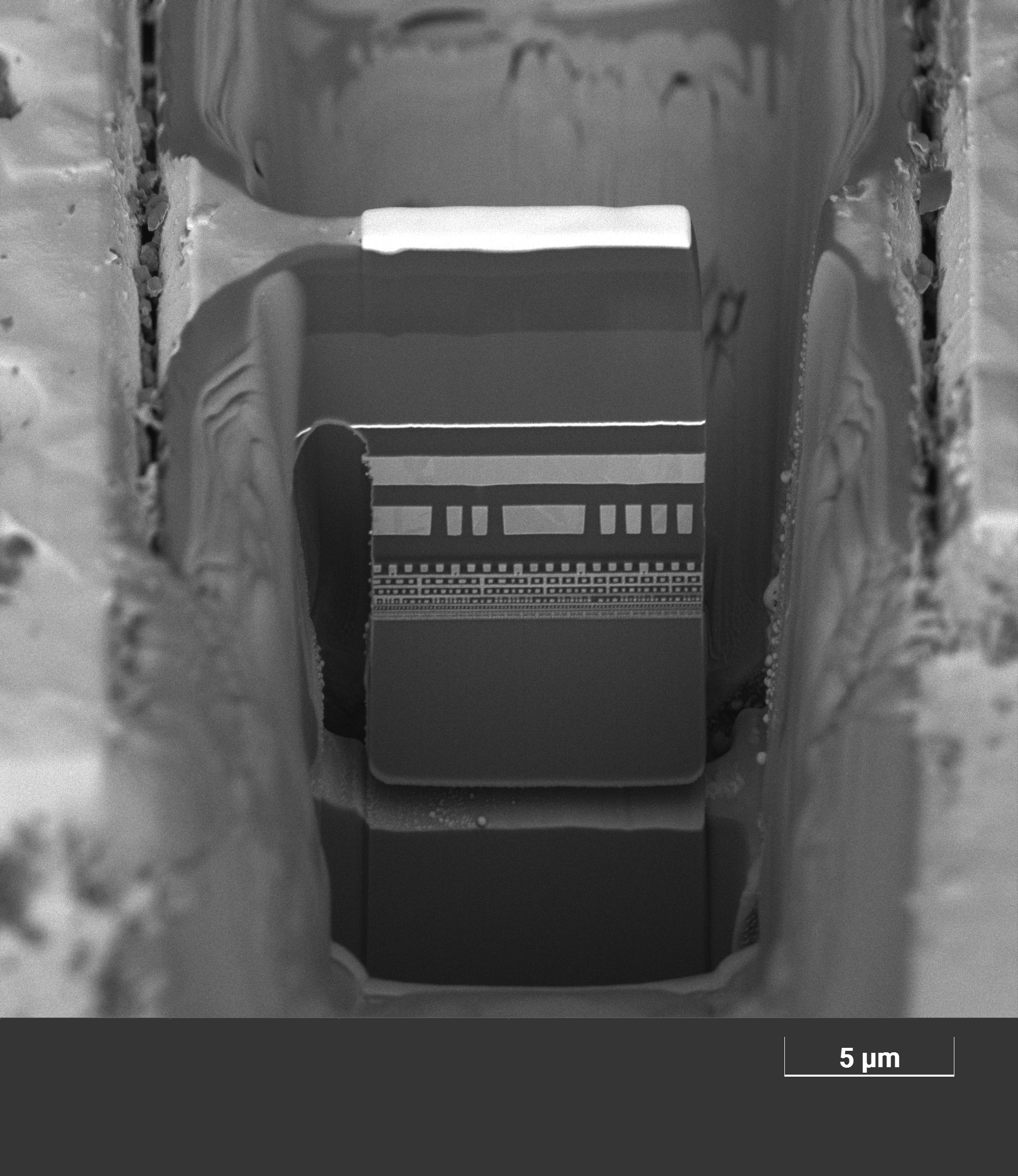
The improved spot profile of Orage™ 2 at high beam currents delivers up to 40% faster milling for TEM lamella preparation, making high-volume work more efficient and reducing the cost per sample. At the same time, clearer low-keV FIB imaging down to 500 eV ensures precise beam placement during the final cleaning step, helping users avoid the “gray-in-gray” effect and giving them full confidence in achieving ultra-thin lamellae.
With Orage™ 2 at its core, FIB-SEM Tescan SOLARIS™ 2 builds on these advantages to accelerate fully automated lamella preparation by almost half. Automation is driven by the TEM AutoPrep™ Pro software module, which reduces operator effort by managing every step from trench milling and lift-out to the final low-keV clean on the grid. During the lift-out step, Tescan’s OptiLift™ attaches the lamella to the grid in a single, reliable motion. Together, they create a seamless, fully automated workflow for top-down, inverted, and planar geometries, perfectly suited for demanding semiconductor applications such as 3D NAND and FinFETs.
test video
Contextual advertising can be profitable. It can either pay for your hosting and maintenance costs for you website or it can pay for a lot more.
Low keV performance
With market-leading FIB imaging quality down to 500 eV, Orage™ 2 gives you maximum visibility of the finest details of your lamella. This clarity enables confident cleaning of ultra-thin lamellae (<10nm) with negligible amorphization damage and makes precise beam placement easier, ensuring smooth completion of the final polishing steps during TEM sample preparation.
AI-powered automated workflow
The AI-driven automated lamella preparation reduces human error, shortens training time, and enables reliable unattended operation even for demanding semiconductor applications. The automation is realized through the TEM AutoPrep™ Pro software module and the OptiLift™ nanomanipulator, forming a fully integrated system that delivers fast lamella preparation while ensuring consistent quality.
Up to 40% faster TEM lamella preparation
The improved spot profile at high beam currents allows lamella preparation to be completed up to 40% faster compared to conventional solutions. This improves efficiency across every lab, whether you’re a researcher, failure analysis, or quality control engineer.
Reliable outcomes
Proven fully automated lamella preparation, combined with long-term column stability and a well-defined beam spot profile, ensures reliable FIB performance across multiple unattended runs and delivers consistent, reproducible results.
This is more than information; it's an advantage. We've compiled our technical whitepapers, detailed product flyers, and on-demand webinars to provide you with the knowledge that makes a real difference. Sign up now to access the insights you need to make an impact.
|
Source |
Gallium liquid metal ion source
|
|
Ion source lifetime |
min. 3000 μAh
|
|
Apertures
|
30 piezo-motorized apertures
|
|
Ion beam energy range |
500 eV – 30 keV
|
|
Probe current |
< 1 pA–100 nA
|
|
Maximum field of view |
1 mm @ 10 keV
|
|
Ion Beam Resolution
|
2.5 nm @ 30 keV
230 nm @ 500 eV |
|
Source |
Gallium liquid metal ion source
|
|
Ion source lifetime |
min. 3000 μAh
|
|
Apertures
|
30 piezo-motorized apertures
|
|
Ion beam energy range |
500 eV – 30 keV
|
|
Probe current |
< 1 pA–100 nA
|
|
Maximum field of view |
1 mm @ 10 keV
|
|
Ion Beam Resolution
|
2.5 nm @ 30 keV
230 nm @ 500 eV |
No distributors found.