Back to the events
Tescan will exhibit at the International Symposium for Testing and Failure Analysis (ISTFA), October 4-8, 2026, in San Antonio, Texas.
Organized by ASM International, ISTFA brings together the semiconductor failure analysis community to share the latest methodologies, technologies, and best practices.
Visit Tescan at Booth #605 to explore semiconductor workflows for defect localization, cross-sectioning, high-resolution imaging, and root cause analysis.

ISTFA is an annual symposium focused on semiconductor testing, reliability, and failure analysis, bringing together researchers and industry professionals to discuss analytical techniques and semiconductor workflows.
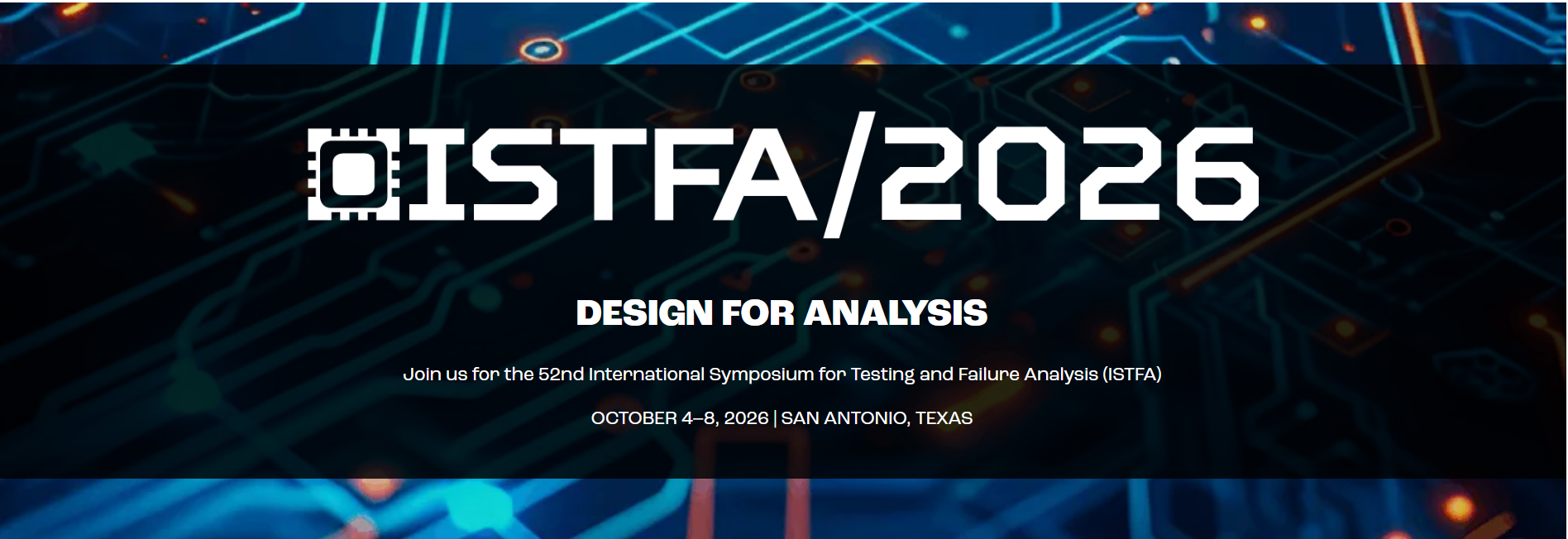
Tescan will exhibit at ISTFA 2026, presenting demonstrations and semiconductor failure analysis workflows under the theme “See the Failure. Solve the Problem.”
Tescan will showcase technologies including:
- Tescan FemtoChisel™ Laser – Femtosecond laser preparation for rapid, low-damage cross-sectioning and access to regions of interest.
- Tescan SOLARIS™ – Plasma FIB-SEM for semiconductor cross-sectioning, sample preparation, and 3D characterization.
- Tescan AMBER X™ 2 – Xe plasma FIB-SEM for TEM specimen preparation, serial sectioning, and semiconductor failure analysis.
- Tescan TENSOR™ S/TEM – Automated S/TEM for high-resolution imaging, diffraction, spectroscopy, and 4D-STEM analysis.
Together, these technologies support semiconductor workflows from defect localization and site-specific sample preparation to high-resolution imaging and root cause analysis.
These systems support advanced semiconductor workflows for:
- Defect localization
- FIB-SEM sample preparation
- Site-specific cross-sectioning
- High-resolution SEM imaging
- Failure analysis and root cause investigation
- Semiconductor process and packaging analysis
Visit Booth #605 to discuss practical approaches to semiconductor failure analysis and workflow efficiency with the Tescan team.
Scientific Presentations
Tuesday, October 6, 2026 | 3:20 PM | Bridge Hall
- From Access to Insight An AI-Based End-to-End Failure Analysis Pipeline Combining Laser Sample Prep, Correlative Navigation, and Automated Image Analytics Presented by Dr. Pouya Tavousi
Wednesday, October 7, 2026 | 3:00-4:00 PM | Exhibit Hall Poster Session
-
High-Throughput Laser Sample Preparation and Device De-processing with LPL and Intelligent Multigas Processing, Reserving FIB for Final High-Resolution Steps Presented by Dr. Pouya Tavousi
- Enabling Efficient Strain Analysis of Advanced Nodes with STEM Nanobeam Diffraction Enhanced by Beam Precession at Sub-2nm Spatial Resolution Presented by Dr. Daniel Nemecek
What You Will Learn
- Semiconductor failure analysis workflows
- Methods for precise defect localization and navigation
- FIB sample preparation and cross-sectioning
- High-resolution SEM imaging for nanoscale structures
- Faster, consistent FA workflows
- Practical applications for logic, memory, advanced packaging, and power devices
- Techniques for improving imaging quality and analytical consistency
Who Should Attend
- Semiconductor failure analysis and reliability engineers
- Microscopy and materials specialists
- Semiconductor and advanced packaging researchers
- Lab managers, technical leaders, and academic researchers
Why Attend
ISTFA brings together researchers and industry professionals to discuss semiconductor testing, reliability, and failure analysis. Visit Tescan to explore integrated workflows for defect localization, FIB sample preparation, SEM imaging, and root cause analysis.
Registration
Registration information and the full event program are available through the official ISTFA event website hosted by ASM International

Visitors are invited to meet the Tescan team at Booth # 605 to discuss semiconductor failure analysis workflows and microscopy solutions for advanced device characterization.