About IPFA 2026 – IEEE Symposium on Failure Analysis
Tescan will present an integrated semiconductor failure analysis workflow for advanced packaging:
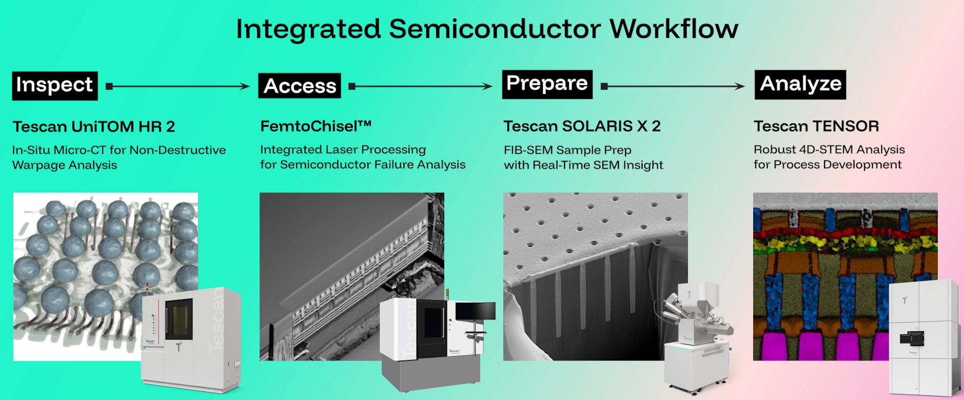
The workflow connects non-destructive 3D inspection, laser-based access, Plasma FIB-SEM sample preparation, and downstream nanoscale analysis.
Agenda / Programme
Tescan FemtoChisel™: Next-Generation Gas-Assisted Femtosecond Laser Workflows for Advanced Microelectronics
Monday, 13 July 2026 | 17:00–17:30
Session: WA2
Speaker: Hervé Macé
Location: Breakout Room A, MELATI Main 4001AB–4002
Novel High-Quality High-Throughput Femtosecond Laser Cross-Sectioning for Advanced Microelectronics Failure Analysis and Metrology
Wednesday, 15 July 2026 | 10:00–10:30
Session: 1A.4, ID259
Speaker: Dr. Sina Shahbazmohamadi
Location: Breakout Room A, MELATI Main 4001AB–4002
Scalable Laser Micromachining Workflows for TEM and NanoCT Sample Preparation
Thursday, 16 July 2026 | 10:20–10:40
Session: 4B.4, ID261
Speaker: Dr. Sina Shahbazmohamadi
Location: Breakout Room B, MELATI Main 4101AB–4102
What You Will Learn
- How correlative workflows combine micro-CT, laser processing, and Plasma FIB-SEM for advanced packaging failure analysis
- How non-destructive 3D imaging supports inspection and localization before physical sample preparation
- How femtosecond laser cross-sectioning can support high-throughput failure analysis and metrology workflows
- How laser micromachining can be applied to TEM and NanoCT sample preparation
- How FIB-SEM workflows support precise preparation and analysis of complex semiconductor samples
- How an integrated Inspect → Access → Prepare → Analyze workflow can reduce workflow complexity in package-level FA
Why Attend
Advanced packages contain buried structures, complex interfaces, and features that require careful correlation between inspection, access, preparation, and analysis. Tescan’s IPFA 2026 programme focuses on practical workflows for package-level failure analysis, including non-destructive 3D imaging, femtosecond laser processing, Plasma FIB-SEM preparation, and nanoscale analytical methods.
Registration
Visit Tescan at Booth A4 during IPFA 2026 to discuss your failure analysis and sample preparation challenges with our technical team.
Meet our experts at IPFA 2026 - Book a meeting with Tescan.
Mr. Herve Mace
Global Business Development Director, Tescan
Hervé Macé is Global Business Development Director for Semiconductors at Tescan and Deputy General Manager of the Laser Technologies BU (Storrs/CT/USA), focusing on advanced workflows for semiconductor applications. At IPFA 2026, he contributes to discussions on microscopy and sample preparation, supporting integrated approaches to failure analysis and advanced packaging. His work focuses on aligning analytical technologies with practical challenges in semiconductor manufacturing and diagnostics.
Dr. Sina Shahbazmohamadi
Head of Laser Technology, Tescan
Dr. Sina Shahbazmohamadi is Head of Technology at Tescan, focusing on translating advanced engineering developments into practical solutions for semiconductor and materials science applications. At IPFA 2026, he presents on femtosecond laser processing and scalable workflows for high-throughput failure analysis and sample preparation in advanced microelectronics. His work bridges innovation and application, supporting efficient and reproducible analytical workflows.
.png?width=107&height=26&name=Tescan(Logo).png "Tescan(Logo)")