WEBINAR | Tailored Cryo-EM and Correlative Workflows for Challenging Biological Projects

Tescan TENSOR

4D-STEM for Semiconductors

TENSOR-2
TENSOR-2

Achieve precise strain mapping, phase orientation analysis, and high-throughput compositional characterization with Tescan TENSOR™. 

This integrated analytical STEM platform with synchronized EDS and precession-assisted 4D-STEM systems is designed for advanced semiconductor device analysis. It delivers sub-2 nm resolution of precession-assisted 4D-STEM measurements, real-time data visualization, and fully automated beam alignment for consistent, reproducible results.

TENSOR™ delivers clarity, speed, and reliability across applications ranging from FinFET strain analysis to 3D NAND grain size mapping.
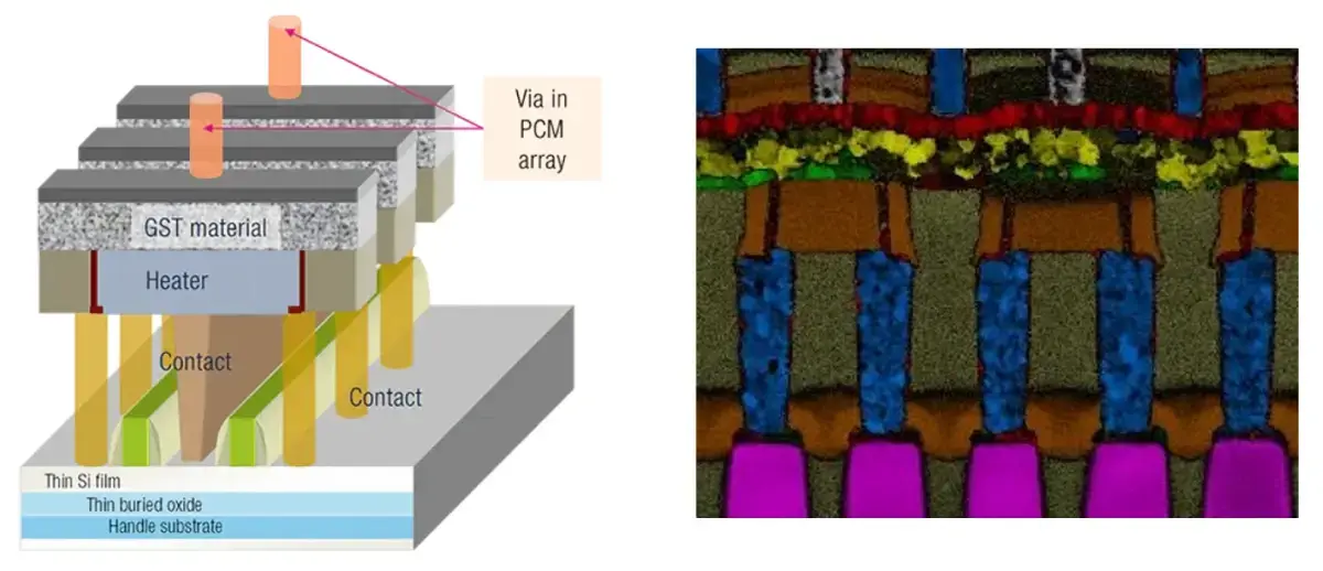
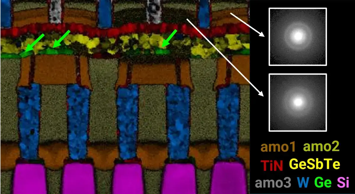
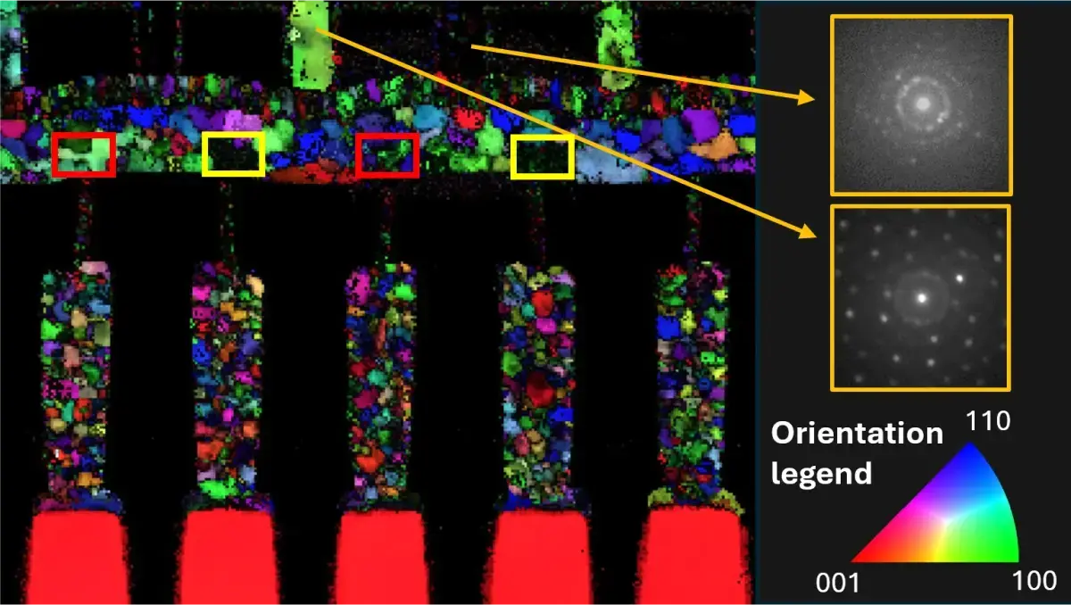
  • Integrated STEM imaging, EDS elemental analysis, and 4D-STEM mapping enhanced by beam precession in one platform

  • Real-time, interactive 4D-STEM and elemental analysis with immediate visualization of processed results in the Explore™ software

  • Automated alignment and tilt-to-zone-axis for reproducible results

  • Near-UHV conditions to protect samples from contamination

  • High-throughput acquisition with direct electron detector, Dectris Quadro, for crisp electron diffraction and 2.0 sr solid angle for efficient EDX data collection

  • Sub-2 nm resolution strain analysis for FinFET and nanosheet GAA architectures

  • Sub-2nm resolution phase-orientation mapping for fine grains in deposited layers

How Tescan TENSOR™ Enables Advanced 4D-STEM Analysis

Accelerate 4D-STEM Data Acquisition

Capture diffraction and EDS datasets in minutes instead of hours with high-speed beam precession, 100 kV electron acceleration, direct electron detection, and 2.0 sr collection solid angle for EDX signals.

Achieve Sub-2 nm resolution of Strain and Phase-Orientation Mapping

Resolve fine structural details in FinFETs, nanosheets, and 3D NAND devices for accurate strain engineering, process development, and defect analysis.

Automate Beam Alignments and Tilt to the Zone-Axis

Eliminate manual adjustments with fully automated alignments and tilt-to-zone-axis procedure for consistent, accurate, and reproducible results.

Protect Samples with Near-UHV Conditions

Prevent hydrocarbon contamination during extended analysis for uncompromised data quality and repeatable measurements.

Unify STEM, EDS, and Precession Diffraction

Streamline multimodal analysis in a single platform to correlate structural, chemical, and phase data efficiently.

Process and Visualize Data in Real Time with Explore™

Access live diffraction and elemental maps during acquisition for immediate interpretation and faster decision-making.

Software Overview

Explore™
 The central interface for STEM imaging, EDS compositional analysis and mapping, precession diffraction, and 4D-STEM workflows. Process data on-the-fly and visualize results in real time with live overlays, pattern matching, and mapping tools—shortening the path from acquisition to actionable insight.
Unlocked content

Unlock 
tescan insight

leave a contact to access

Get the most out of Tescan

This is more than information; it's an advantage. We've compiled our technical whitepapers, detailed product flyers, and on-demand webinars to provide you with the knowledge that makes a real difference. Sign up now to access the insights you need to make an impact.

TESCAN TENSOR™ for Semiconductors

Technical specification
TENSOR

Accelerating Voltage:  100 kV (optimized for high scattering contrast and dose-limited resolution)

STEM Resolution: 2.8 Å

Beam Precession Frequency: Up to 72,000 Hz

Diffraction Detector: Direct Electron (DED)
- maximum frame rate 4,500 fps
- dynamic range ~10⁷ 

EDS System: Dual windowless detectors with 2.0 sr solid angle

Vacuum System: Near-UHV vacuum in sample area (<10⁻⁶ Pa)

Beam Blanking: Integrated electrostatic blanker, 1 MHz rate

Precession Angle Range: 0.1° to 3.0°

Automation Features: Beam alignments, Tilt to the zone axis, Measurement presets

TENSOR_1-1

GET IN Touch

with specialist

map

Where can you find us:

Tescan
Libušina třída 21
623 00 Brno
Czech Republic

130405923 us US 37.09024 -95.712891 25.3575 29.349345 20.67957527 42.082797 39.91384763 -33.693421 13.93320106 3.039986586 31.997988 38.050985 47.579533 30.052597 48.1485965 58.375799 54.663142 19.195447 56.975106 47.916997 50.493053 45.868592 10.79556993 44.35660598 43.2371604 55.536415 14.557577179752773 32.100937 -6.116829 -6.212299277967318 33.600194 -12.08688 23.7104 -33.471062 31.998740087 -23.69149395 43.462349 51.529848 49.1893523 49.197486 25.072375 31.075811 1.299027 40.676979 52.30150662 51.013813 35.684121 37.566531 52.246622 40.581349 39.911632 -26.1811371 41.818215 33.429928

No distributors found.