Tescan TENSOR™ with Precession-Assisted 4D-STEM
Tescan TENSOR™ combines high-resolution STEM imaging with precession-assisted 4D-STEM diffraction and elemental analysis. This is all within the intuitive Tescan Essence™ interface.
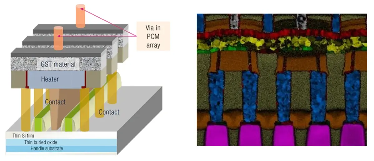
You can capture imaging, diffraction, and phase data in real time without switching tools. This enables fast orientation mapping, crystallization analysis, and phase segregation detection in PCM devices.
- Precession-assisted 4D-STEM: reduces dynamical scattering for accurate phase and strain measurements
- Integrated STEM-diffraction interface: perform imaging, diffraction, and orientation mapping in a single workflow
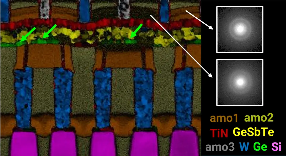
- Virtual dark field imaging: generate contrast-sensitive maps to distinguish crystalline vs amorphous regions
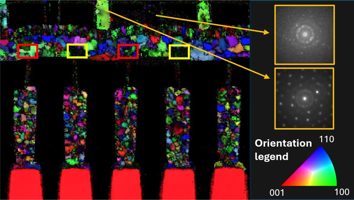
- Orientation mapping tools: visualize grain boundaries and GST grain orientations with nanometer precision
- Automated cross-correlation routines: ensure reproducible phase and orientation analysis across large datasets