Deliver Reliable Sub-10 nm Delayering
Achieve uniform, artifact-free results with Nanoflat, Chase, and C-Maze chemistries designed for advanced nodes.
Uncover the electrical and structural details of today’s most advanced devices with Tescan AMBER X 2 Plasma FIB-SEM. Purpose-built for semiconductor applications, AMBER X 2 combines Xe plasma FIB with proprietary Nanoflat, Chase, and C-Maze chemistries to deliver uniform, artifact-free delayering at sub-10 nm nodes.
The system ensures you have reproducible workflows across logic, memory, and I/O regions, supporting electrical fault isolation, failure analysis, and transistor-level probing.
Deliver Reliable Sub-10 nm Delayering
Achieve uniform, artifact-free results with Nanoflat, Chase, and C-Maze chemistries designed for advanced nodes.
Preserve Device Integrity
Maintain electrical properties during preparation with low-kV Xe Plasma FIB milling and inert ions.
Control Processes with Confidence
Rely on end-point detection and live monitoring to stop precisely at the target layer.
Connect Workflows Seamlessly
Combine automated delayering and in situ nanoprobing in one Plasma FIB-SEM system.
Access Planar I/O Layers
Ensure flat, reproducible deprocessing of thick metal and I/O regions using low-angle polishing with a clamp holder.
Resolve Clarity at Every Scale
Resolve transistor-level details with BrightBeam™ UHR SEM optics at sub-500 eV.
Use Tescan AMBER X 2 with Mistral plasma FIB to perform Sub-20 nm node delayering that enables precise endpoint detection and in-situ nanoprobing of advanced transistors.
Apply Tescan Low Angle Polishing with in-column BSE monitoring to control real-time delayering and visualize metal-via transitions layer by layer.
Combine TRUE X-sectioning with Rocking Stage to achieve curtaining-free, wide-area cross-sections for fast and reliable semiconductor failure analysis.
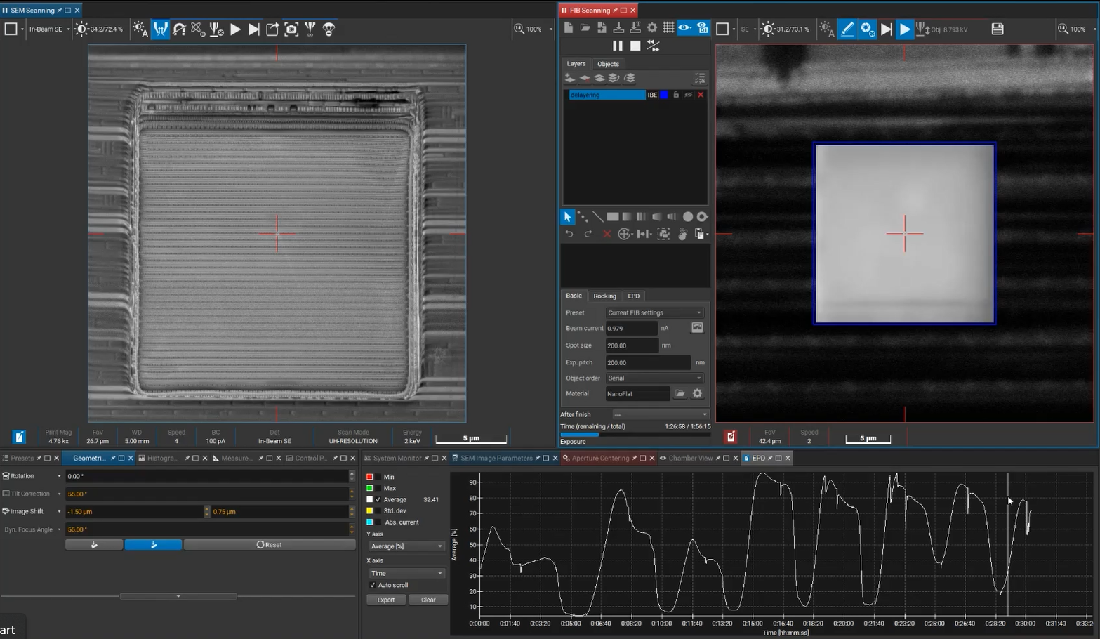
Tescan AMBER X 2 is designed to work seamlessly with the Tescan Delayering™ module. Automated recipe control and factory-defined templates let you carry out repeatable delayering across logic, memory, and I/O regions, reducing operator variability and ensuring consistent results.
The system integrates advanced monitoring tools, including end-point detection and live signal tracking, so you can stop precisely at the target layer without over- or under-milling. Proprietary Nanoflat, Chase, and C-Maze chemistries are optimized within the software, giving you reproducible outcomes at sub-10 nm nodes.
For challenging applications, AMBER X 2 supports low angle polishing with a dedicated clamp holder, delivering planar deprocessing of thick metal and I/O layers. Together, these capabilities streamline semiconductor workflows, helping you move efficiently from delayering to imaging and in situ nanoprobing in a single Plasma FIB-SEM platform.
This is more than information; it's an advantage. We've compiled our technical whitepapers, detailed product flyers, and on-demand webinars to provide you with the knowledge that makes a real difference. Sign up now to access the insights you need to make an impact.
|
SEM
|
Resolution: Ultra-high resolution at sub-100 eV with BrightBeam™ optics |
|---|---|
|
Imaging modes: Secondary electrons, BSE, Passive Voltage Contrast SEM |
|
|
FIB Preparation Process
|
Ion source: Mistral™ Xe+ plasma ion source (ECR type), source lifetime not limited |
|
Max current: >3.3 µA at 30 keV for high-throughput large-area milling |
|
|
Low keV capability: Gentle delayering to preserve device integrity |
|
|
Delayering chemistries: Nanoflat, Chase, and C-Maze for uniform removal |
|
|
Automation & Control
|
Software: Tescan Delayering™ module with factory-defined recipes |
|
Monitoring: Live end-point detection and real-time signal tracking |
|
|
Workflow integration: Seamless transition to in situ nanoprobing |
|
|
Sample Handling
|
Stage: Compucentric 5-axis motorized stage |
|
Optional: Piezo XYZ sub-stages of 3rd party nanoprobing platforms Tescan for probing geometry control |
|
|
Holder: Dedicated clamp holder for low angle polishing of I/O layers |
|
|
Nanoprobing & Characterization
|
Applications: PMOS/NMOS transistor probing, EFA-ready workflows |
|
Integration: In situ nanoprobing within the same platform |
|
|
Contrast imaging: Passive voltage contrast SEM for electrical inspection |
|
SEM
|
|---|
|
Resolution: Ultra-high resolution at sub-100 eV with BrightBeam™ optics |
|
Imaging modes: Secondary electrons, BSE, Passive Voltage Contrast SEM |
|
FIB Preparation Process
|
|---|
|
Ion source: Mistral™ Xe+ plasma ion source (ECR type), source lifetime not limited |
|
Max current: >3.3 µA at 30 keV for high-throughput large-area milling |
|
Low keV capability: Gentle delayering to preserve device integrity |
|
Delayering chemistries: Nanoflat, Chase, and C-Maze for uniform removal |
|
Automation & Control
|
|---|
|
Software: Tescan Delayering™ module with factory-defined recipes |
|
Monitoring: Live end-point detection and real-time signal tracking |
|
Workflow integration: Seamless transition to in situ nanoprobing |
|
Sample Handling
|
|---|
|
Stage: Compucentric 5-axis motorized stage |
|
Optional: Piezo XYZ sub-stages of 3rd party nanoprobing platforms Tescan for probing geometry control |
|
Holder: Dedicated clamp holder for low angle polishing of I/O layers |
|
Nanoprobing & Characterization
|
|---|
|
Applications: PMOS/NMOS transistor probing, EFA-ready workflows |
|
Integration: In situ nanoprobing within the same platform |
|
Contrast imaging: Passive voltage contrast SEM for electrical inspection |
Tescan
Libušina třída 21
623 00 Brno
Czech Republic
No distributors found.