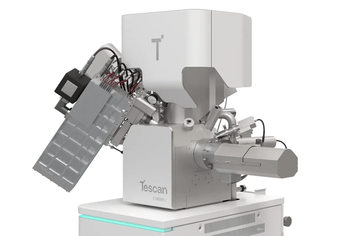
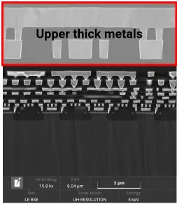
Achieve Curtaining-Free Delayering of Upper Metal Layers with Tescan Low Angle Polishing 

Apply Tescan Low Angle Polishing with in-column BSE monitoring to control real-time delayering and visualize metal-via transitions layer by layer.

Low_Angle_Polishing_for_delayering_of_upper_thicker_layers
Unlocked content

Tescan solutions

Control Layer-by-Layer Deprocessing with Curtaining-Free Low Angle Polishing

Thick I/O stacks and upper metal layers in advanced semiconductor nodes are notoriously difficult to deprocess with orthogonal FIB methods. Curtaining, non-uniform surfaces, and uncertain endpoints often obscure critical device features and limit reliability in analysis.

Tescan Essence™ Low Angle Polishing uses plasma FIB at shallow tilt angles with automated multi-angle rotation to achieve uniform, curtaining-free surfaces. In-column BSE monitoring provides real-time visualization of metal-via transitions, enabling precise, reproducible layer-by-layer deprocessing at 14 nm and beyond.

Why Use Low Angle Polishing Workflows for Delayering Thick I/O and Upper Metal Layers?

Delayer I/O Regions with Thick Metal Interconnects

1_Delayering of Input-Output area with thick metal lines

Remove upper metal layers cleanly using plasma FIB at low tilt angles. Expose the I/O region without curtaining artifacts, ensuring uniform surfaces ready for further structural analysis.


Achieve Uniform Layer Removal with Low Angle Polishing

2_Low Angle Polishing FIB milling strategy

Apply plasma FIB milling from four directions to prevent curtaining artifacts. Ensure consistent material removal across the I/O area for reliable delayering.


Remove Upper Metal Layers with Uniform Precision

3_Low Angle Polishing of upper thicker metals of semiconductor device

Use low-angle polishing to eliminate thickness-related artifacts. Produce smooth, reproducible surfaces through upper interconnect stacks.


Visualize Cross-Sections Through Multiple Metal Layers

4_Cross-sectional view of semiconductor device across all metal lines (1)

Capture SEM cross-sections that reveal the full vertical stack. Identify both metal and via layers for accurate structural analysis.


Stabilize Samples for Reliable Low Angle Milling

5_Dedicated clamp holder for maximum sample planarity

Secure specimens with a dedicated clamp holder during polishing. Maintain planarity for consistent plasma FIB milling across the I/O region.

Contents 

01

Root of the problem

02
Materials and Methods
03
 Results and Discussion 

1. Root of the Problem

Why Orthogonal FIB Struggles in Delayering Thick I/O and Upper Metal Layers

Accurate semiconductor failure analysis depends on clean, uniform deprocessing. Yet standard orthogonal FIB approaches often fail when applied to thick I/O stacks and upper interconnect layers.

Curtaining artifacts, uneven removal, and uncertain endpoints obscure device features and complicate analysis. Non-planar structures and passivation layers add further challenges, making reproducibility difficult and slowing workflows.

Tescan Essence™ Low Angle Polishing overcomes these limitations with a plasma FIB strategy that combines low-angle incidence, automated multi-angle rotation, and real-time BSE monitoring. The result is smooth, curtaining-free surfaces that preserve structural fidelity and enable controlled, layer-by-layer deprocessing.

  • Low-angle plasma FIB minimizes curtaining in thick I/O stacks
  • Automated four-direction polishing ensures reproducible surfaces
  • In-column BSE monitoring provides real-time endpoint detection
  • Uniform delayering of non-planar and passivation layers
  • Reliable workflows reduce operator variability and improve efficiency

Gain full control over upper layer deprocessing and achieve consistent results with Tescan Low Angle Polishing.

2. Materials and Methods

How Low Angle Polishing Was Applied to Delayer Thick I/O and Upper Metal Layers

A semiconductor device containing a thick I/O region was selected to demonstrate low angle plasma FIB polishing. Initial localization of the area of interest was performed in SEM mode, with in-column BSE imaging used to evaluate surface morphology and identify layer transitions.

Plasma FIB milling was then performed at a shallow tilt angle of 2–4°, combined with automated four-direction stage rotation. This ensured uniform ion beam exposure and minimized curtaining artifacts during material removal.

Real-time BSE monitoring within the Tescan Essence™ interface provided live visualization of metal and via transitions, with intensity plots guiding endpoint detection and layer control. SEM image logging was used throughout the process for documentation and verification.

The integrated workflow enabled smooth, reproducible delayering of upper metal layers and passivation regions, producing clean cross-sections suitable for failure analysis and structural characterization.

3. Results and Discussion

Curtaining-Free Delayering Enables Reliable Analysis of Upper Metal Stacks

Tescan Essence™ Low Angle Polishing produced smooth, uniform surfaces across the I/O region, even in thick upper interconnect layers. Plasma FIB milling at low tilt angles with automated four-direction rotation eliminated curtaining artifacts that normally obscure structures.

Real-time in-column BSE monitoring provided continuous visibility of metal–via transitions, enabling precise endpoint detection and controlled removal of individual layers. Intensity plots confirmed reproducible layer-by-layer deprocessing at the 14 nm node.

SEM images logged throughout the workflow verified uniform surface quality and showed that non-planar structures and passivation regions were polished without distortion. Compared to orthogonal FIB methods, low angle polishing improved reproducibility, reduced operator dependency, and preserved structural fidelity.

This workflow demonstrates clear advantages for semiconductor failure analysis and process verification, delivering consistent results across complex I/O stacks and reliable access to underlying device layers.

Unlock 
tescan insight

leave a contact to access

Get the most out of Tescan

This is more than information; it's an advantage. We've compiled our technical whitepapers, detailed product flyers, and on-demand webinars to provide you with the knowledge that makes a real difference. Sign up now to access the insights you need to make an impact.

Tescan Instruments & Technology

Used in This Workflow

Tescan AMBER X – Plasma FIB-SEM 

A unique plasma FIB-SEM combining a Xenon plasma FIB with a field-free UHR SEM column, enabling high-throughput milling and high-resolution imaging. Tescan AMBER™ X is ideal for delayering thick I/O regions and upper interconnect stacks, delivering curtaining-free surfaces that preserve device structures for further analysis.


  • Xenon plasma FIB: ensures efficient, large-area material removal

  • Ultra-high-resolution SEM imaging: verifies surface quality during delayering

  • Field-free design: allows precise imaging of delicate structures without distortion 
AMBER-X2

Tescan Essence™ Low Angle Polishing (LAP) Module 

A dedicated software module that extends plasma FIB workflows with shallow-angle incidence and automated four-direction rotation. The Essence™ LAP module enables smooth, reproducible delayering of thick I/O and non-planar regions, while integrated in-column BSE monitoring ensures accurate layer-by-layer endpoint detection.


  • Low-angle incidence: eliminates curtaining artifacts in thick I/O stacks

  • Automated four-angle rotation: produces uniform, reproducible surfaces

  • In-column BSE monitoring: provides real-time visibility of metal–via transitions

  • SEM image logging: ensures complete documentation and verification

GET IN Touch

Contact us

map

Where can you find us:

Tescan Brno
Libušina třída 21
623 00 Brno 
Czech Republic

info@Tescan.com