Reproducible Nanometer-Scale Imaging
Achieve consistent, ultra-high-resolution results across users and sessions with BrightBeam™ technology and In-Flight Beam Tracing™, ensuring stable beam conditions and repeatable imaging quality.
Achieve consistent, ultra-high-resolution imaging and fast EDS analysis across diverse materials with Tescan MIRA XR™. Gain reliable results through advanced beam stability, intelligent automation, and adaptable vacuum modes to make every workflow precise, efficient, and easy to manage.
Reproducible Nanometer-Scale Imaging
Achieve consistent, ultra-high-resolution results across users and sessions with BrightBeam™ technology and In-Flight Beam Tracing™, ensuring stable beam conditions and repeatable imaging quality.
Confident Imaging of Challenging Samples
Capture reliable images of charging, porous, or beam-sensitive materials in MultiVac™ low-vacuum mode. No coating is required.
Fast, Accurate Chemical Mapping
Double your EDS throughput with Dual Essence™ EDS, providing precise multi-element maps and reduced shading for efficient compositional analysis.
Streamlined and Automated Workflows
Simplify complex imaging tasks with VisualCoder™ automation, allowing intuitive drag-and-drop workflow creation that reduces operator time by up to 80%.
Effortless Navigation Across Scales
Move seamlessly from large-area overviews to nanoscale details with Wide Field Optics™, accelerating orientation and reducing time-to-data.
EBSD-Ready Crystallographic Analysis
Combine large-area and nanoscale EBSD mapping in one workflow, supported by Tescan MIRA XR™’s stable beam conditions and wide analytical chamber for comprehensive crystallographic studies.
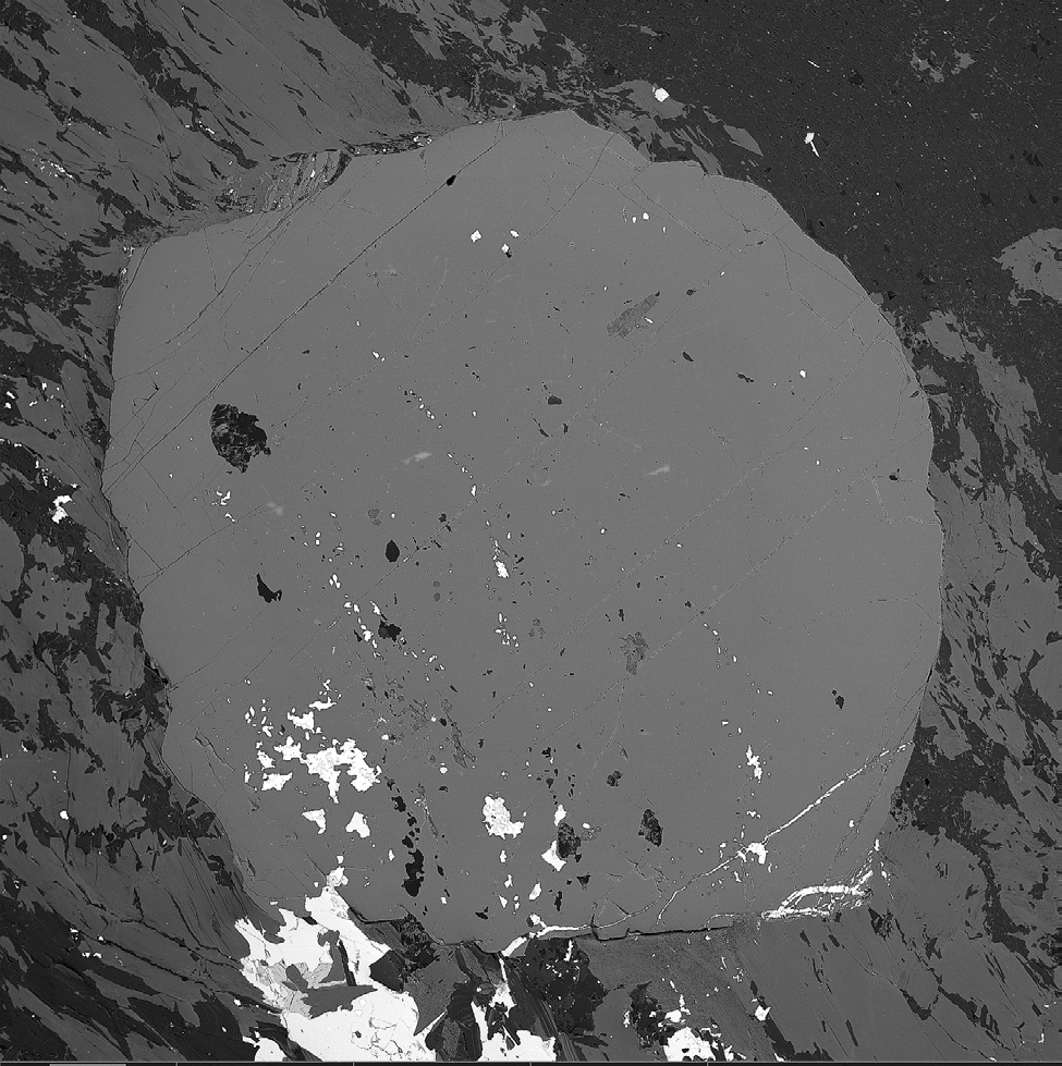
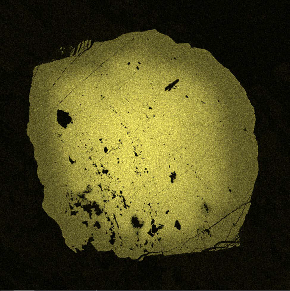
Use Tescan SEMs with Dual Essence™ EDS to perform integrated SEM-EDS analysis that resolves zonation and overlapping phases in complex geological samples.
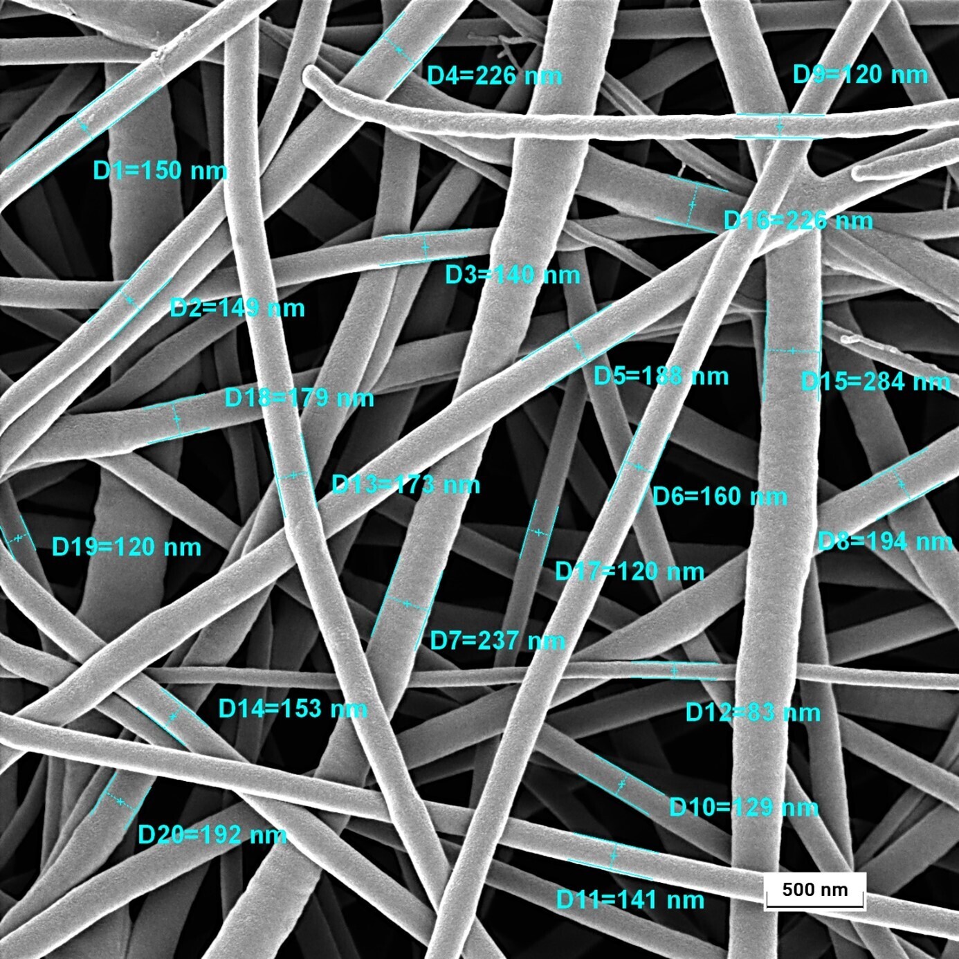
Tescan MIRA XR™ enables non-destructive imaging of fiber morphology and diameter across polymer meshes.
Tescan MIRA XR™ provides high-resolution insight into SBA-15 particle shape and structure.
AUTOMATED IMAGE ACQUISITION FOR REPRODUCIBLE MATERIALS ANALYSIS
Essence™ Image Snapper automates image collection across multiple regions of interest, ensuring every dataset is captured under consistent, optimized conditions. Integrated into the Essence™ environment, it reduces operator input and speeds up data acquisition for morphology, composition, and defect analysis.
With unattended batch routines, Image Snapper delivers reproducible, high-quality SEM images for standardized materials research and quality control.
It also supports panorama creation, automatically stitching images into seamless large-area overviews. This is ideal for studying microstructural uniformity and contextualizing nanoscale features within broader sample regions.
This is more than information; it's an advantage. We've compiled our technical whitepapers, detailed product flyers, and on-demand webinars to provide you with the knowledge that makes a real difference. Sign up now to access the insights you need to make an impact.
|
Tescan MIRA XR™ UHR SEM-EDS for Materials Science
Specifications shown are based on the GM chamber configuration. |
Ultra-high resolution BrightBeam™ FE-SEM column |
|---|---|
|
Resolution: |
|
|
Magnification range from 1× to 2,000,000× |
|
|
Essence™ integration for SEM and EDS in one interface |
|
|
Elemental mapping, line scans, and point analysis included |
|
|
Wide Field Optics™ for SEM navigation from 1× |
|
|
Essence™ 3D Collision Model for chamber visualization and protection |
|
|
MultiVac low vacuum imaging up to 500 Pa |
|
|
5-axis motorized stage with max sample size of 335 × 280 × 133 mm³ and load capacity up to 8 kg |
|
|
20+ chamber ports ready for detector upgrades |
|
|
Included & Optional Accessories
|
Dual Essence™ EDS detectors for high-speed mapping |
|
In-Column Axial detector for high-efficiency ultra-high resolution imaging |
|
|
EBSD detector for crystallographic analysis from large maps to nanoscale |
|
|
STEM detector for transmission imaging at sub-nanometer resolution |
|
|
VisualCoder™ and SEM Expert PI for workflow automation and customization |
|
|
VisualCoder for workflow automation and SEM Expert PI for advanced automation and scripting |
|
Tescan MIRA XR™ UHR SEM-EDS for Materials Science
Specifications shown are based on the GM chamber configuration. |
|---|
|
Ultra-high resolution BrightBeam™ FE-SEM column |
|
Resolution: |
|
Magnification range from 1× to 2,000,000× |
|
Essence™ integration for SEM and EDS in one interface |
|
Elemental mapping, line scans, and point analysis included |
|
Wide Field Optics™ for SEM navigation from 1× |
|
Essence™ 3D Collision Model for chamber visualization and protection |
|
MultiVac low vacuum imaging up to 500 Pa |
|
5-axis motorized stage with max sample size of 335 × 280 × 133 mm³ and load capacity up to 8 kg |
|
20+ chamber ports ready for detector upgrades |
|
Included & Optional Accessories
|
|---|
|
Dual Essence™ EDS detectors for high-speed mapping |
|
In-Column Axial detector for high-efficiency ultra-high resolution imaging |
|
EBSD detector for crystallographic analysis from large maps to nanoscale |
|
STEM detector for transmission imaging at sub-nanometer resolution |
|
VisualCoder™ and SEM Expert PI for workflow automation and customization |
|
VisualCoder for workflow automation and SEM Expert PI for advanced automation and scripting |
Tescan
Libušina třída 21
623 00 Brno
Czech Republic
No distributors found.