
For large-scale cross-sectioning and delayering of heterogeneous materials, Tescan FemtoChisel™ uses true femtosecond laser processing to deliver material removal rates up to 2,000× faster than Xe plasma FIB and up to 10,000× faster than Ga FIB. This boosts lab productivity while reducing time-to-sample and cost-per-sample.
Submit Your Sample for Advanced Contrast SEM Analysis
Join a Collaborative Study in Advanced Contrast SEM (Scanning Electron Microscopy)
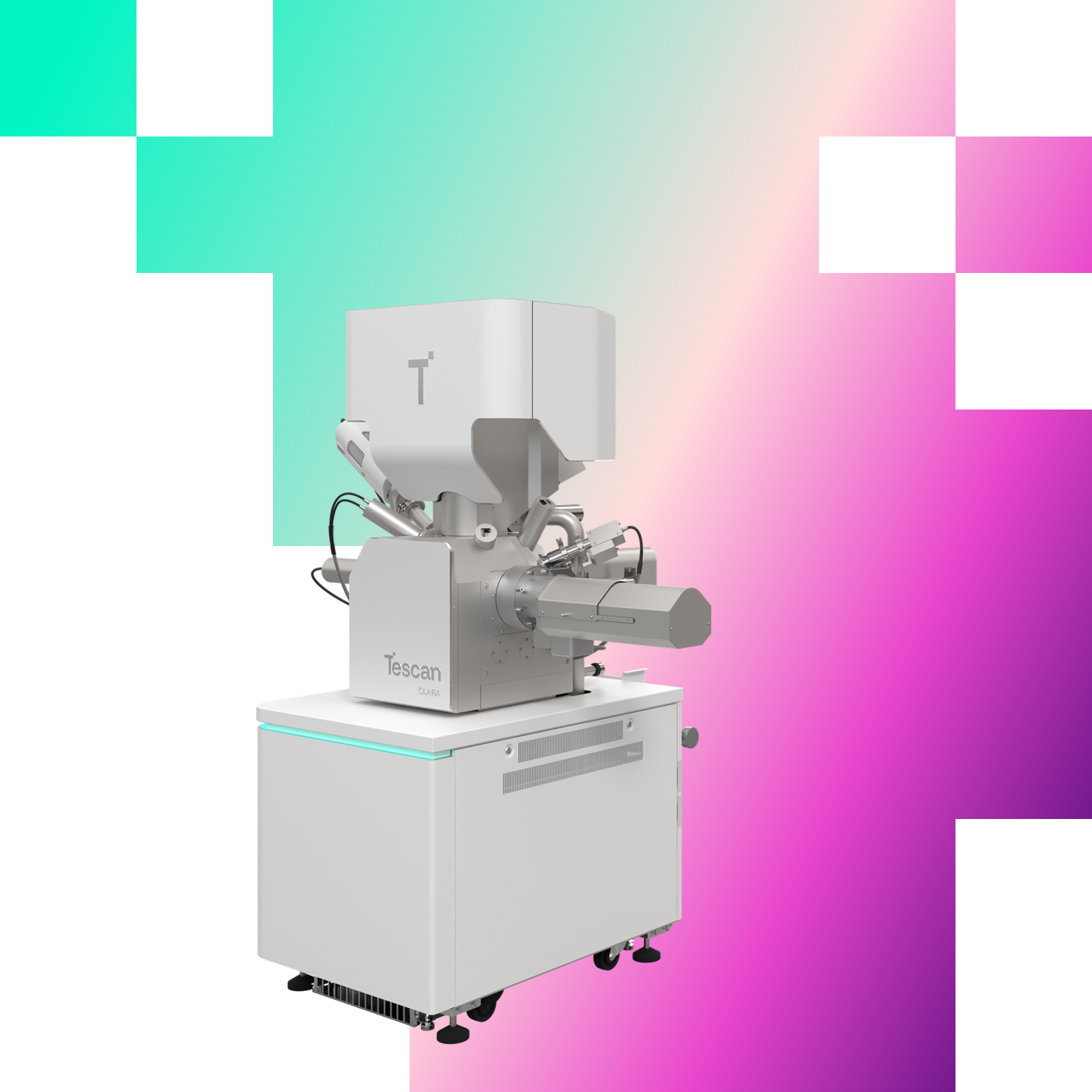
Be part of a collaborative imaging study exploring how advanced SEM contrast can reveal details that conventional imaging may miss.
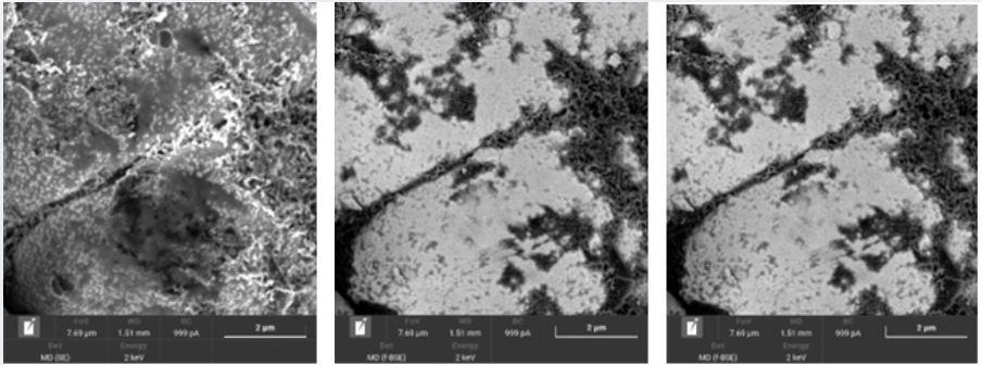
Submit your sample for evaluation using our full suite of detectors and imaging modes on the new Tescan CLARA™ . Our specialists will analyze your material and show how complementary signals from the same region can reveal surface details, material differences, and subtle features that are often missed in standard imaging.
Want to see the difference for yourself? Submit your sample for advanced SEM analysis.
This service is intended for samples where advanced backscattered electron signal selectivity can uncover additional insight beyond conventional SEM observation.
What Makes a Sample Suitable?
To ensure meaningful results, submitted samples must include:
- Fine‑Scale Structure
Nanoscale to sub-micron features
Very large, uniform, or fully homogeneous samples are less likely to benefit from this analysis.
- Clear Material or Contrast Variation
More than one material, phase, or composition, or local variations that can be distinguished by contrast rather than only topography.
- Surface or near-surface features
Features located on the surface or very close to it, such as thin layers or coatings, fine particles, inclusions, or subtle surface modifications or residues.
- Subtle or Challenging Contrast
Samples where standard BSE imaging shows limited contrast, where small features are difficult to separate from the surrounding material, or additional insight is needed to separate surface effects from bulk material.
OF YOUR SAMPLE ANALYSIS
Suitable samples may include:
-
Multi‑material or nano-composite samples
-
Coated or treated surfaces with small defects
-
Sintered, porous, or powder‑based materials with contaminations
-
Samples with suspected surface contamination or segregation
A strong candidate for this analysis is a material with a substrate and a nanometer-scale particle covered with nanoparticles of different materials. One example is a battery cathode with a carbon binder, where surface particles and features are well below 50 nm and located directly at the surface.
For samples like this, we can isolate surface contrast by collecting backscattered electrons from the outermost particles, revealing fine details that are otherwise impossible to distinguish in conventional imaging.
.png?width=201&height=200&name=_%20Application%20area%20icon%20(3).png)
Tescan FemtoChisel™ in Semiconductors
High-precision laser micromachining for semiconductor sample preparation and failure analysis
- Adaptive multi-material processing, with proprietary intelligent multi-gas processing and laser protective layer that preserve device integrity across metals, polymers, and advanced packaging stacks.
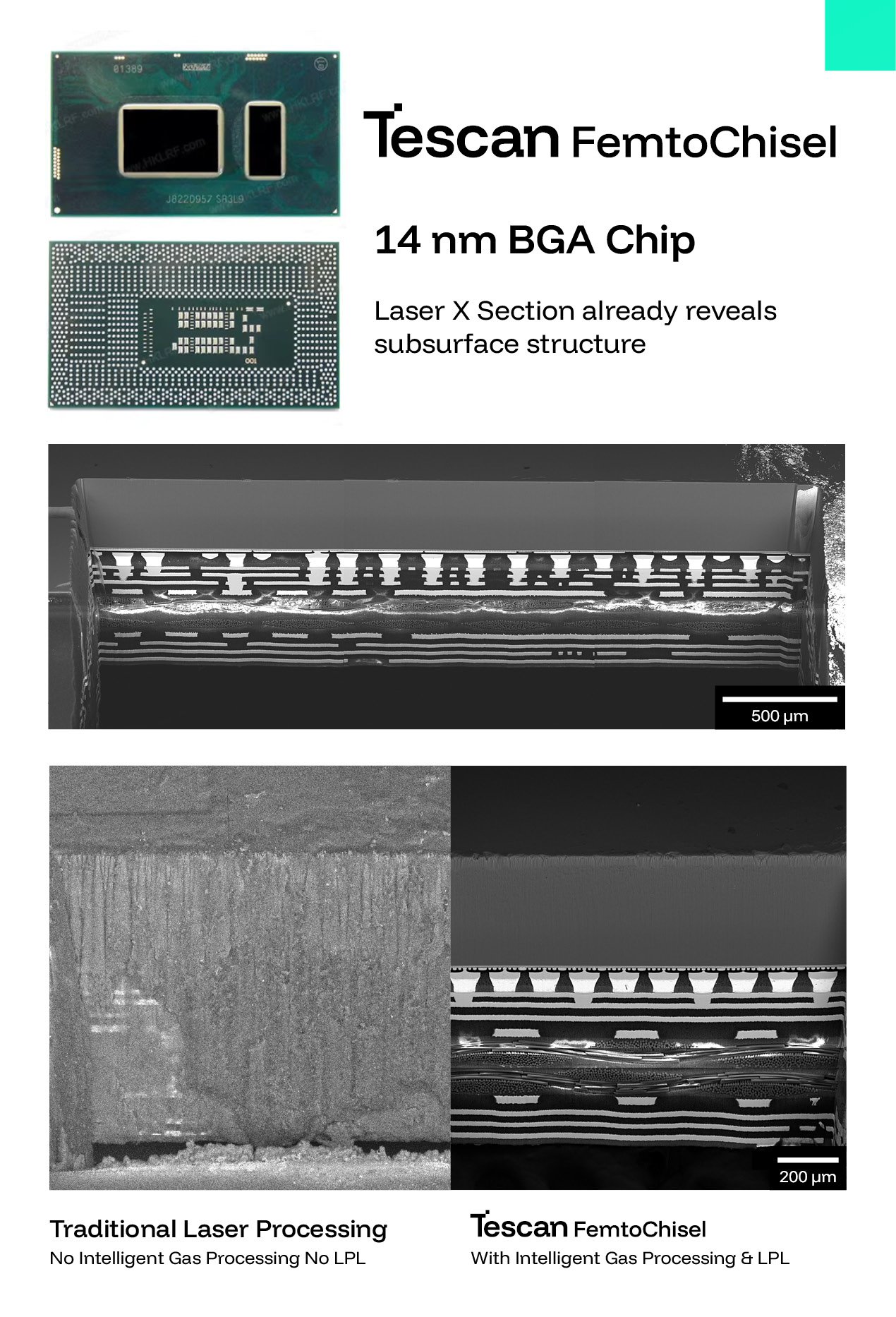
- High-throughput access to buried structures with taper-corrected, debris-free cross-sections – often eliminating the need for post FIB polishing.
- Selective backside thinning with mirror-like surfaces (Ra < 0.4 µm), enabling optical fault analysis without artifacts.
- Large-area delayering (5–10 mm) with automated endpointing for accurate layer-by-layer removal at laser speeds.
- By uniting laser processing, electron microscopy, and FIB into complementary workflows, Tescan is helping semiconductor innovators overcome traditional bottlenecks in sample preparation. FemtoChisel™ serves both recipe-driven environments and flexible research in advanced packaging and R&D labs, providing a versatile solution for current and future semiconductor demands.
Tescan FemtoChisel™ accelerates semiconductor workflows that demand speed, precision, and surface integrity. Operating in the non-thermal ablation regime, it enables engineers to access deeply buried regions of interest without microcracks, melt zones, or redeposition. The system delivers reproducible, analysis-ready results across advanced devices, supporting physical failure analysis, process development, and reverse engineering.
OF YOUR SAMPLE ANALYSIS
Suitable samples may include
-
Multi‑material or nano-composite samples
-
Coated or treated surfaces with small defects
-
Sintered, porous, or powder‑based materials with contaminations
-
Samples with suspected surface contamination or segregation
Example of an ideal sample
A strong candidate for this analysis is a material with a substrate and a nanometer-scale particle covered with nanoparticles of different materials. One example is a battery cathode with a carbon binder, where surface particles and features are well below 50 nm and located directly at the surface.
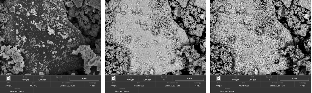 For samples like this, we can isolate surface contrast by collecting backscattered electrons from the outermost particles, revealing fine details that are otherwise impossible to distinguish in conventional imaging.
Technical specification
.png?width=1131&height=979&name=N%C3%A1vrh%20bez%20n%C3%A1zvu%20(1).png)
Advanced SEM Multi‑Detector Analysis