March 19, 2026
Tescan opens new Korea demo lab supporting semiconductor analysis
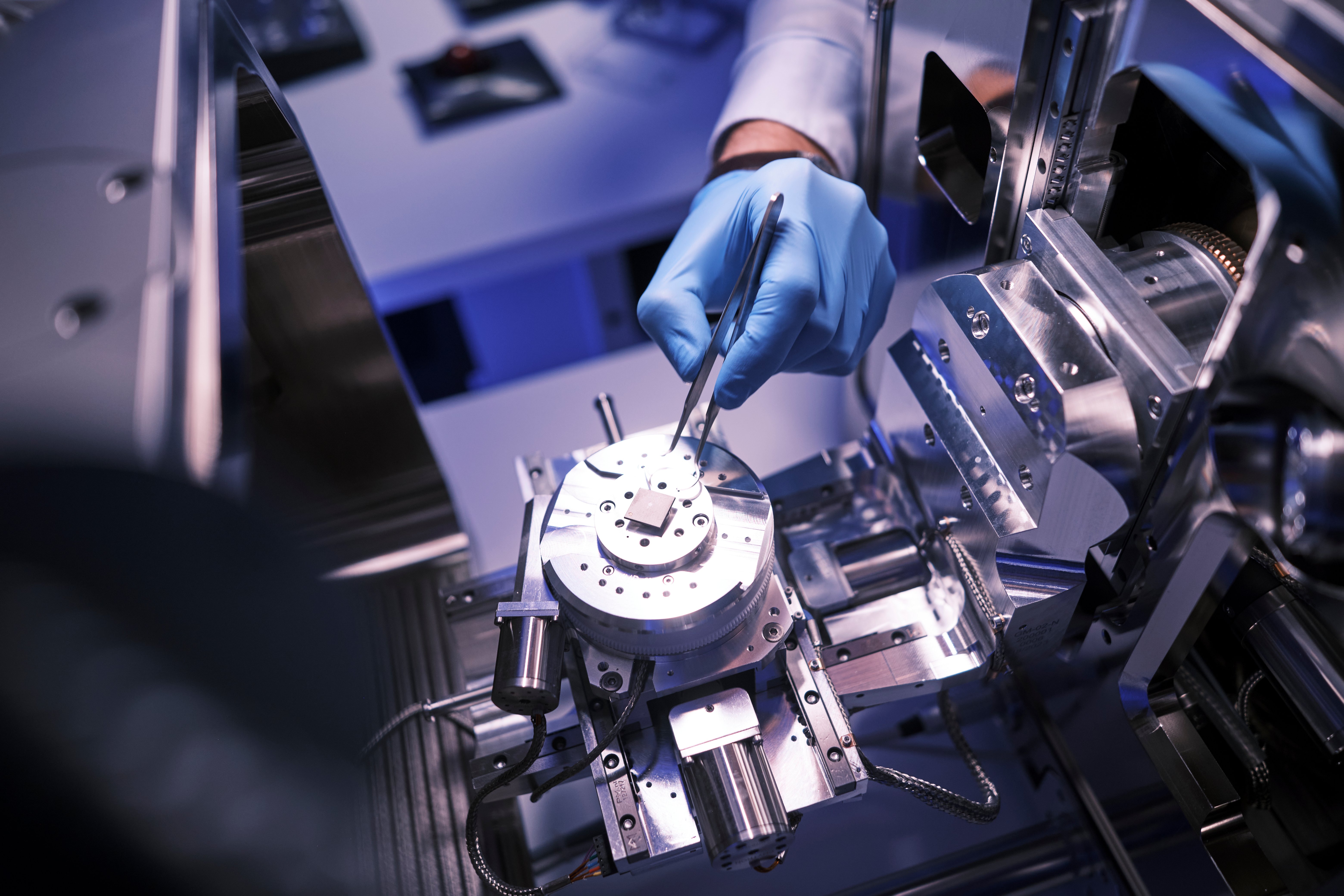
Tescan offers on‑site demos in a new scanning electron microscopy lab in Korea, supporting the semiconductor industry, research institutions and universities with FIB‑SEM expertise.