Defect Localization
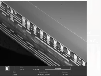
High-resolution SEM imaging and navigation for identifying areas of interest.
High-resolution SEM imaging and navigation for identifying areas of interest.

Advanced FIB and laser-based techniques for cross-sectioning and accessing buried structures.

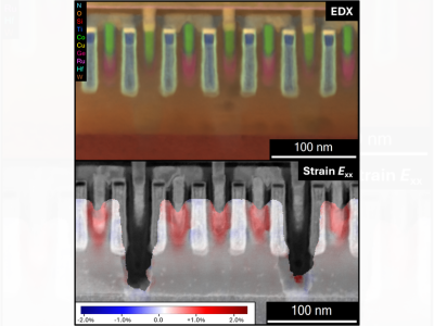
High-resolution imaging and analytical STEM techniques to investigate material structures and failure mechanisms.

Complementary technologies that help reduce time-to-answer while maintaining analytical precision.
12:45 - 13:45
February 27, 2023
12:45 - 13:45
February 27, 2023
12:45 - 13:45
February 27, 2023
12:45 - 13:45
February 27, 2023
12:45 - 13:45
February 27, 2023
12:45 - 13:45
February 27, 2023
February 27, 12:45 - 13:45, LL Copernicum, level 0
February 27, 12:45 - 13:45, LL Copernicum, level 0
February 27, 12:45 - 13:45, LL Copernicum, level 0
February 27, 12:45 - 13:45, LL Copernicum, level 0
February 27, 12:45 - 13:45, LL Copernicum, level 0
February 27, 12:45 - 13:45, LL Copernicum, level 0
12:45 PM - 01:45 PM
February 27, 2023
February 27, 12:45 PM - 01:45 PM, booth 123
Introducing MIRA XR – the analytical SEM reimagined for speed, usability, and ultra-high-resolution imaging. Perfect for analytical workflows across materials science disciplines. Designed to deliver high throughput without compromising on resolution or automation. A productivity platform for every user, from QA labs to advanced research teams.
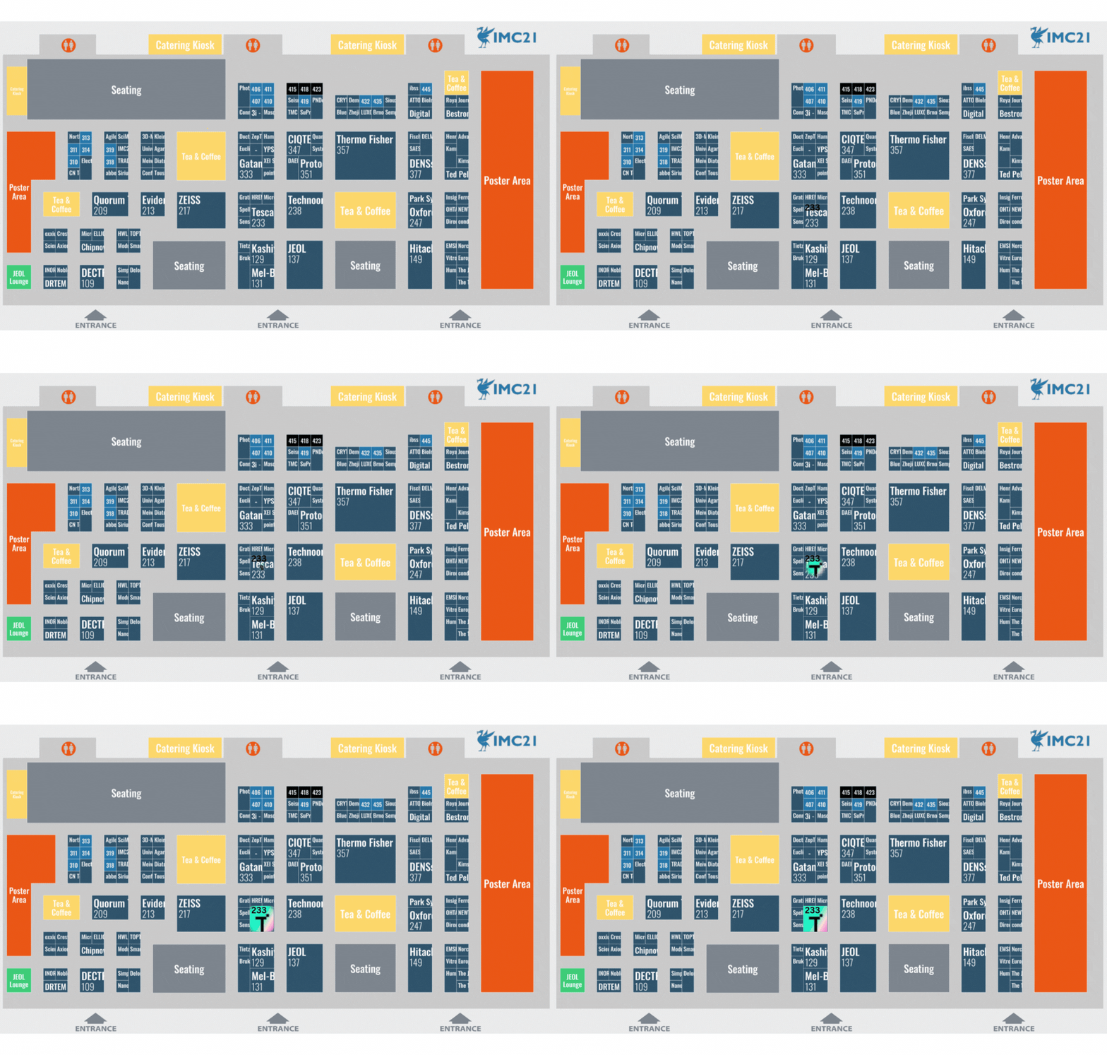
Located at TESCAN's Booth 1324
EXPLORE TESCAN'S INTEGRATED SEMICONDUCTOR FAILURE ANALYSIS WORKFLOW.
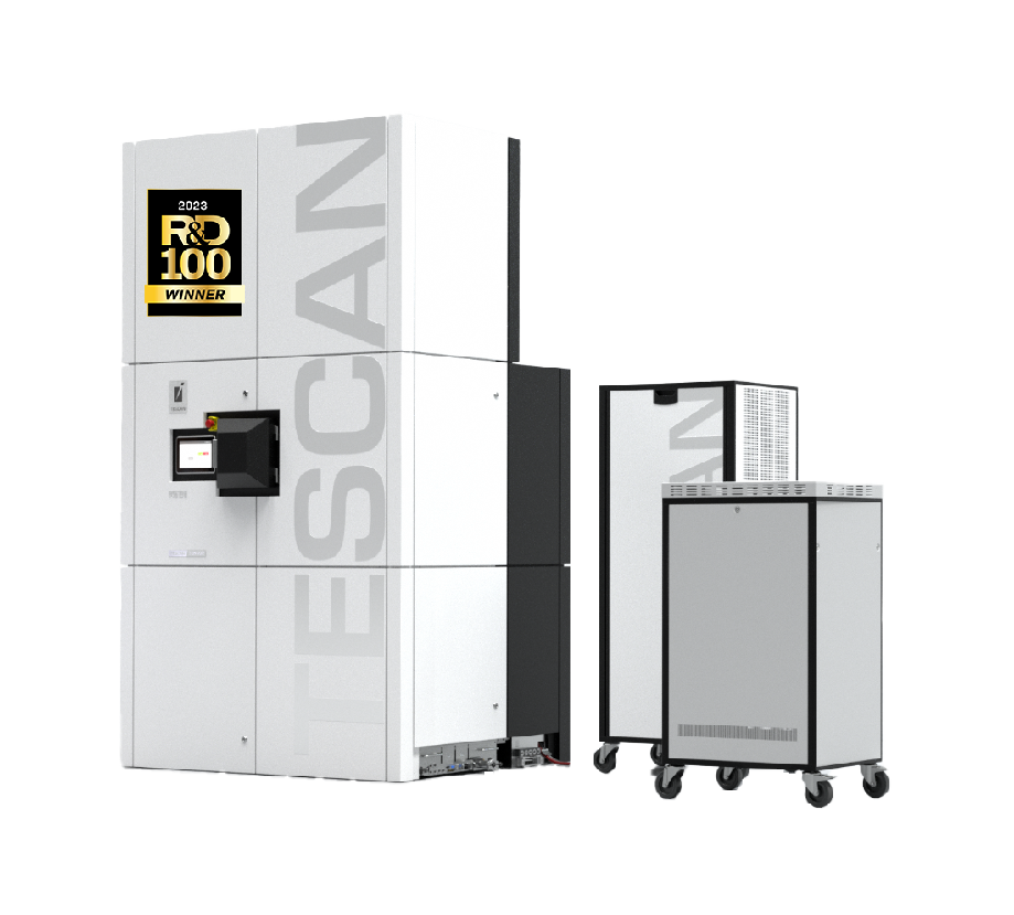
Advanced imaging and analytical characterization, including 4D-STEM, to investigate nanoscale structures and material properties.
You can visit directly at Tescan Booth 414.
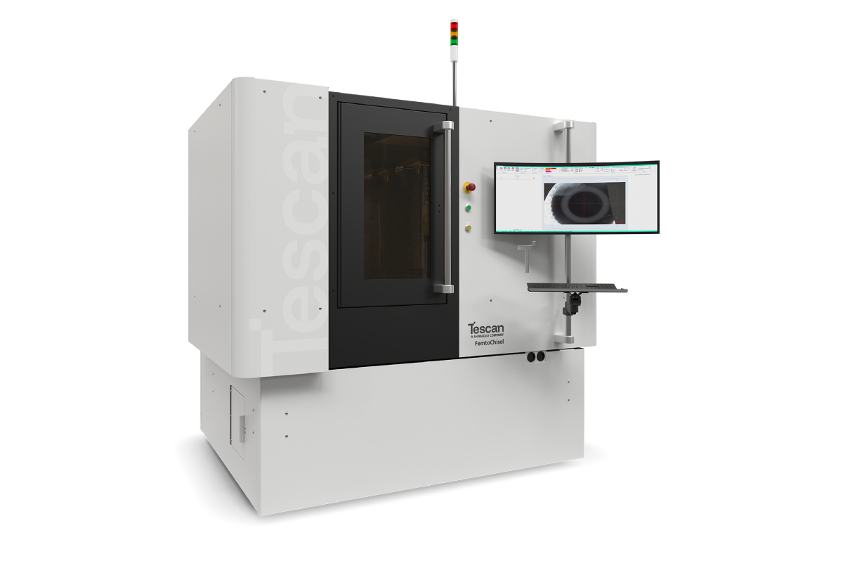
FemtoChisel™ – Femtosecond laser sample preparation
Laser-based material removal for rapid access to buried structures, cross-sectioning, and semiconductor sample preparation.
You can visit directly at Tescan Booth 414.

Large-volume material removal, 3D characterization, and site-specific sample preparation for complex semiconductor structures.
You can visit directly at Tescan Booth 414.
15:20 - 15:40
November 1, 2027

15:00 - 16:00
November 2, 2027

15:00 - 16:00
November 2, 2027
November 1, 15:20 - 15:40, Bridge Hall
November 2, 15:00 - 16:00, Exhibit Hall
November 2, 15:00 - 16:00, Exhibit Hall
Semiconductor Business Development (Global)
Semiconductor Product Marketing
Semiconductor Business Development (North America)

FIB-SEM Business Development (North America)
Head of AI and Advanced Solutions - Laser Solutions
Product Sales Lead - Laser Solutions
Product Sales Lead - STEM Solutions
Vice-President of Sales (Americas)
Sales Manager (US Northwest)

Sales Manager (US Southwest)
Area Sales Director (Singapore)
Area Sales Director (US West & South America)