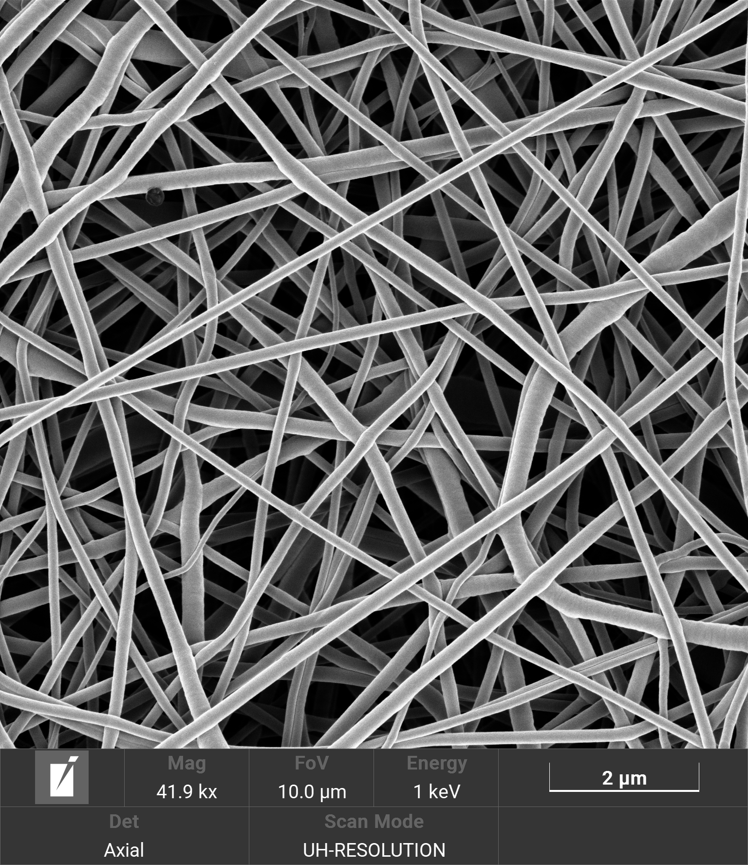
WEBINAR | From Infrastructure to Impact: EM & Micro-CT in Materials Core Facilities

High-Resolution SEM for Quality Assessment of Electrospun Nanofibers

Tescan MIRA XR enables non-destructive imaging of fiber morphology and diameter across polymer meshes.

hero
hero
Unlocked content

When Fiber Quality Comes Down to Nanometers

In electrospinning, subtle changes in process parameters can drastically alter fiber structure, from diameter shifts to the appearance of surface defects or unwanted beads. But without the right analytical tools, these variations can go unnoticed until performance suffers.

Tescan MIRA XR, was used to evaluate polycaprolactone (PCL) nanofiber meshes across a range of electrospinning conditions. High-resolution SEM imaging revealed the impact of polymer concentration and applied voltage on fiber uniformity, enabling rapid, visual feedback for process optimization.

Why Use SEM to Analyze

Electrospun Fibers?

01
Root of the Problem

Diagnosing Defects in Electrospun Materials

Electrospinning is known for its versatile fabrication methods, but that same versatility can be a disadvantage. Humidity, voltage, polymer content, and even spinneret design affect the final material structure. When defects occur, it's often unclear whether they're caused by formulation, process instability, or external contamination.

Polymer nanofiber structures challenge the limits of conventional light microscopy due to their sub-micron diameters and low contrast. While some features may fall within the resolving capability of high-end optical systems, detailed visualization and analysis require a more advanced approach. Scanning electron microscopy (SEM) offers the high spatial resolution and depth of field necessary to characterize fiber morphology, surface texture, and structural uniformity at the nanoscale. However, because nanofibers are often beam- and heat-sensitive, SEM imaging must also be carefully optimized to preserve sample integrity throughout the analysis.

02
Materials and Methods

Visualizing Fiber Morphology with High-Resolution SEM

Electrospun nanofiber meshes made from polycaprolactone (PCL) were imaged using a Tescan MIRA XR SEM, chosen for its ability to operate at low accelerating voltages and provide crisp surface contrast.

Fibers were fabricated with different combinations of polymer concentration and applied voltage. Each sample was imaged at high magnification (5 µm field of view) under beam conditions optimized for low-Z materials. No conductive coating or destructive sample prep was required.

For each image, 20 fibers were measured, and diameter distributions were plotted as box plots. These distributions formed the basis for identifying process settings that minimized bead formation and delivered uniform fiber widths. 

03
Results and Discussion

Structural Domains and Phase Interfaces

High-resolution SEM imaging provided clear visual evidence of how process parameters influence nanofiber formation. The following patterns were observed:

  • Lower polymer concentration = finer, more uniform fibers
    Samples prepared from lower-concentration PCL solutions produced consistent nanofiber meshes with minimal variation in diameter or surface texture.

  • Higher polymer concentration = thicker fibers with reduced uniformity
    As solution concentration increased, fibers became visibly thicker — reaching diameters around 300 nm — and more prone to irregularities.

  • Voltage had a limited effect on fiber size
    Across the tested conditions, applied voltage showed less influence on fiber diameter compared to polymer concentration.

SEM imaging allowed researchers to directly compare fiber meshes, identify inconsistencies, and confirm improvements across iterations.

Thanks to the clarity and speed of the results, SEM quickly became an essential tool in development and quality assurance workflows.

This enabled consistent fiber production at scale — supporting use in biomedical scaffolds, filtration membranes, and other applications where uniformity is critical.

GET IN Touch

Contact us

Get the most out of Tescan

This is more than information; it's an advantage. We've compiled our technical whitepapers, detailed product flyers, and on-demand webinars to provide you with the knowledge that makes a real difference. Sign up now to access the insights you need to make an impact.

Tescan Instruments & Technology

Used in This Workflow

Tescan MIRA XR

A versatile field emission SEM designed for non-destructive surface imaging and fine structural analysis.

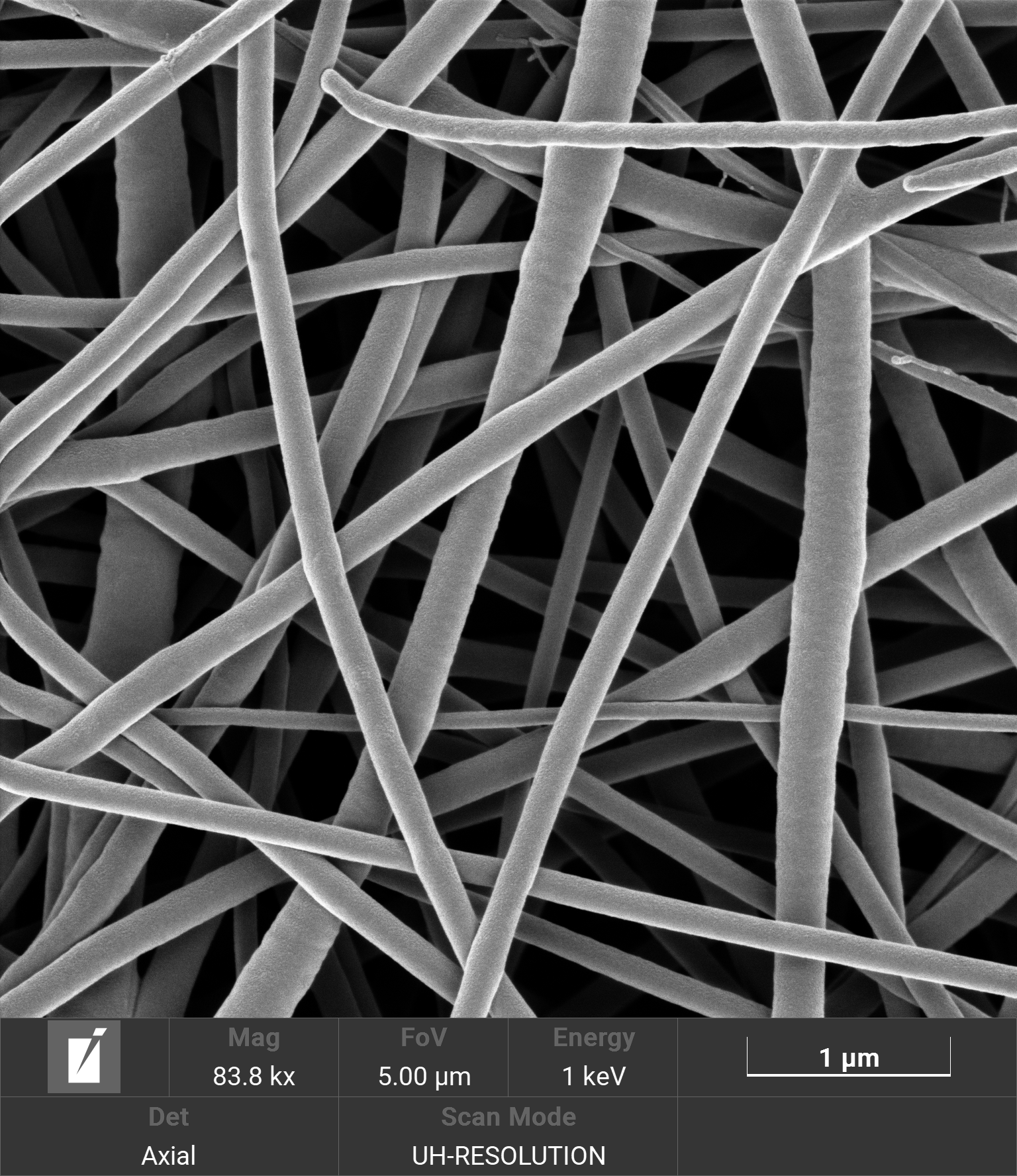
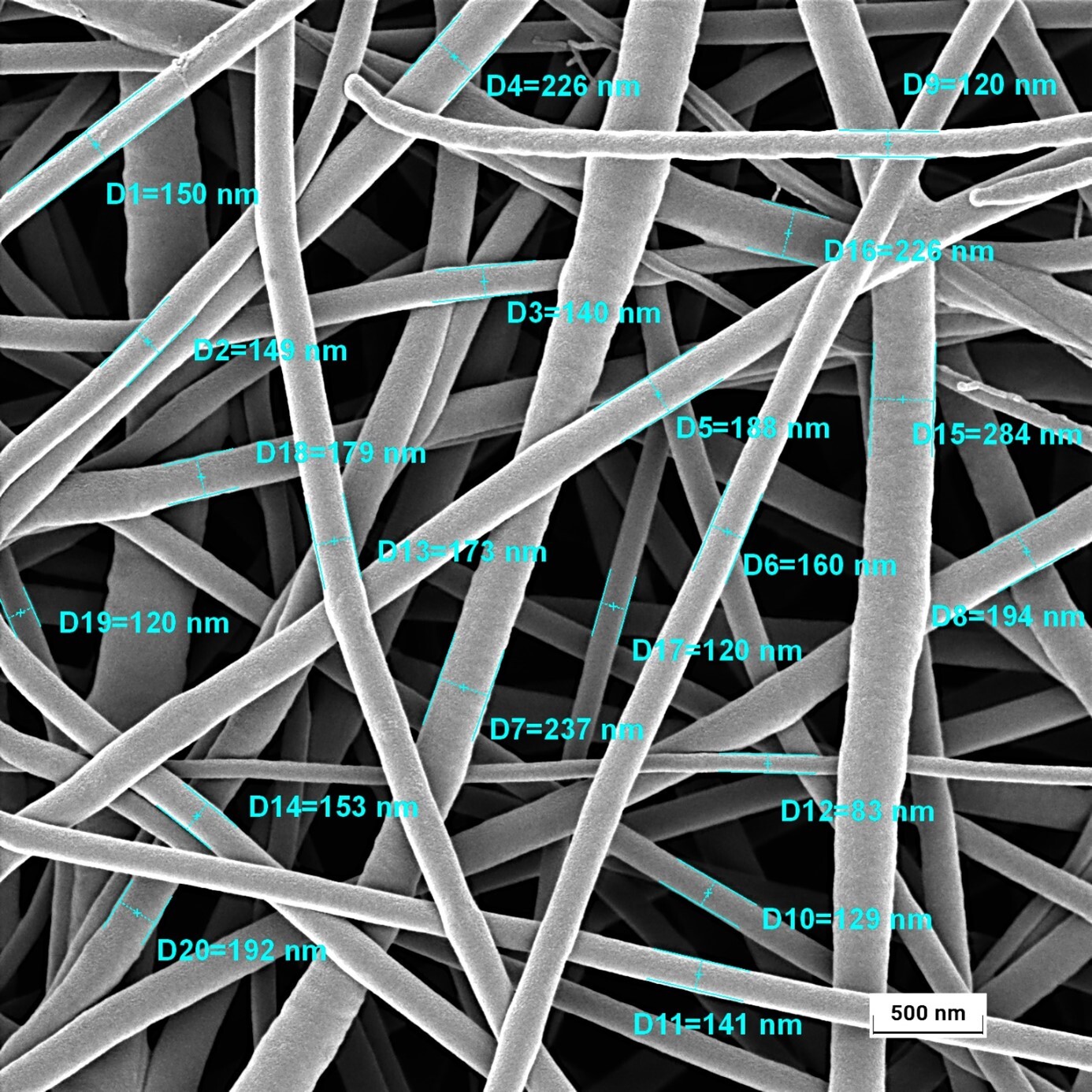
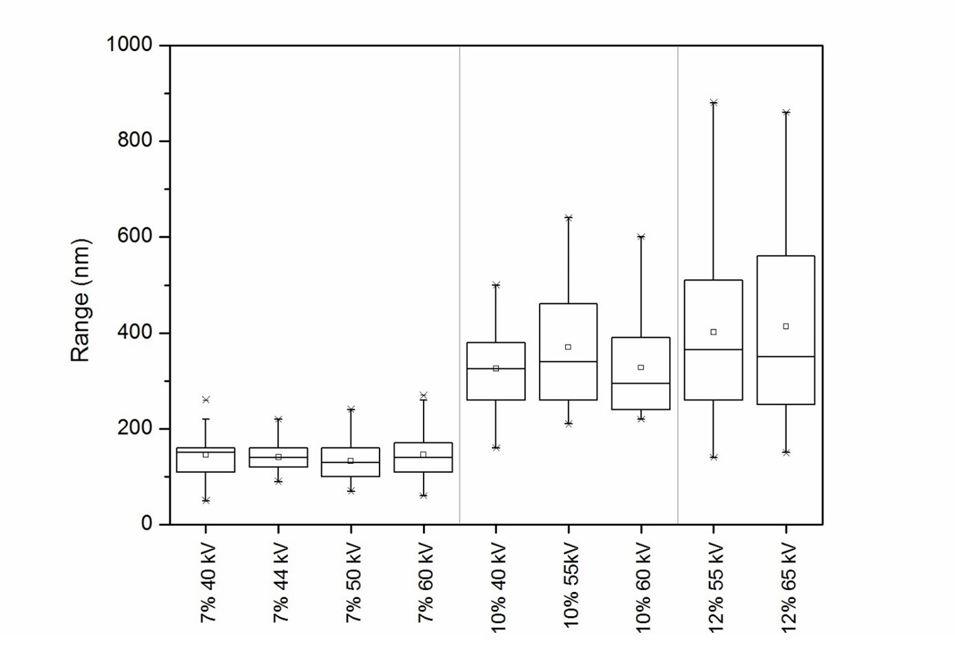
  • Optimized low-kV performance for polymers and other sensitive materials

  • Wide field-of-view spanning macro to nanoscale

  • Ideal for morphology assessment of nanofibers, soft composites, and thin coatings

MIRA XR GM MONO Metal

GET IN Touch

Contact us

map

Where can you find us:

Tescan Brno
Libušina třída 21
623 00 Brno
Czech Republic

info@Tescan.com 

130405923 us US 37.09024 -95.712891 25.3575 29.349345 20.67957527 42.082797 39.91384763 -33.693421 13.93320106 3.039986586 31.997988 38.050985 47.579533 48.1485965 58.375799 54.663142 19.195447 56.975106 50.493053 45.868592 10.79556993 44.35660598 43.2371604 55.536415 14.557577179752773 32.100937 -6.116829 -6.212299277967318 23.7104 -33.471062 31.998740087 -23.69149395 43.462349 51.529848 49.1893523 49.197486 25.072375 31.075811 1.299027 40.676979 52.30150662 51.013813 35.684121 37.479653 52.246622 40.581349 39.911632 -26.1811371 41.818215 33.429928

No distributors found.