WEBINAR | Up to 40% Faster Automated TEM Lamella Preparation with new Ga⁺ FIB Column

Multi-Material Interface Analysis Following Laser Powder Bed Fusion

A hierarchical SEM approach to characterizing the Cu alloy and Fe phase interface.

hero
hero
Unlocked content

Seeing the Interface for What It Is

Joining dissimilar metals in additive manufacturing can unlock unique property combinations, but in systems like Cu–Fe it also pushes metallurgical limits. Different thermal conductivity, melting points, and solidification behavior make the interface the most likely weak point.

In this study, a layered build of Cu₇Ni₂SiCr alloy and nearly pure Fe was produced via laser powder bed fusion (L-PBF). Using a Tescan CLARA UHR SEM with automated panoramic imaging, BSE contrast, EDS, and EBSD, researchers mapped elemental redistribution, grain structures, and phase transitions across the weld zone. These findings help evaluate joint integrity and guide process optimization in multi-material additive manufacturing.

Why Analyze Additive Manufactured Interfaces

with Hierarchical SEM Methodology?

01
Root of the Problem

Dissimilar Metals, Shared Boundaries

L-PBF allows builds that combine Cu₇Ni₂SiCr and Fe for combined strength, conductivity, and magnetic properties. But their low miscibility makes microstructural uniformity difficult. Defects like segregation, porosity, and cracking are common at the fusion line. Rapid solidification can help refine microstructure, but cooling rates and process settings must be tuned carefully.

Understanding how grain structure and elemental gradients form here is critical. Conventional metallography cannot span from macro to micro scale effectively, but SEM-based multimodal workflows can. 

02
Materials and Methods

Automated, Multimodal SEM Workflow

Cu₇Ni₂SiCr (gas-atomized) and Fe (water-atomized) powders were processed by L-PBF. The interface was examined with a Tescan  CLARA UHR SEM using BSE imaging, EDS, and EBSD.

Essence™ Image Snapper stitched 88 BSE fields into a panoramic weld map. EDS quantified elemental gradients and interface widths from Cu and Fe changes.

EBSD phase and IPF maps identified phases, measured grain orientation, and highlighted grain refinement near the interface.

03
Results and Discussion

Structural and Chemical Insights

The panoramic BSE image distinguished Cu-rich and Fe-rich zones with a narrow intermixing band. Higher magnification revealed columnar grains with cellular substructures in Cu, finer equiaxed grains in Fe, and variable interface widths.

EDS confirmed abrupt Cu and Fe changes, with Ni and Si showing gradual gradients that suggest limited diffusion. EBSD showed distinct crystallographic patterns between phases and smaller grains in the interface zone, which may improve strength through dispersion and grain boundary strengthening.

These results connect local solidification behavior and elemental redistribution to weld quality, guiding better process control for multi-material L-PBF.

GET IN Touch

Contact us

Get the most out of Tescan

This is more than information; it's an advantage. We've compiled our technical whitepapers, detailed product flyers, and on-demand webinars to provide you with the knowledge that makes a real difference. Sign up now to access the insights you need to make an impact.

Tescan Instruments & Technology

Used in This Workflow

Tescan CLARA

Combines sub-nanometer resolution with advanced analytics.

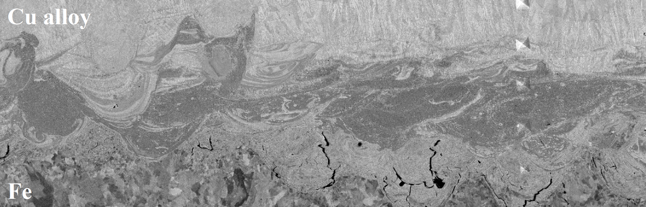
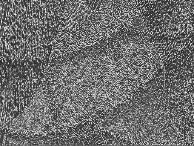
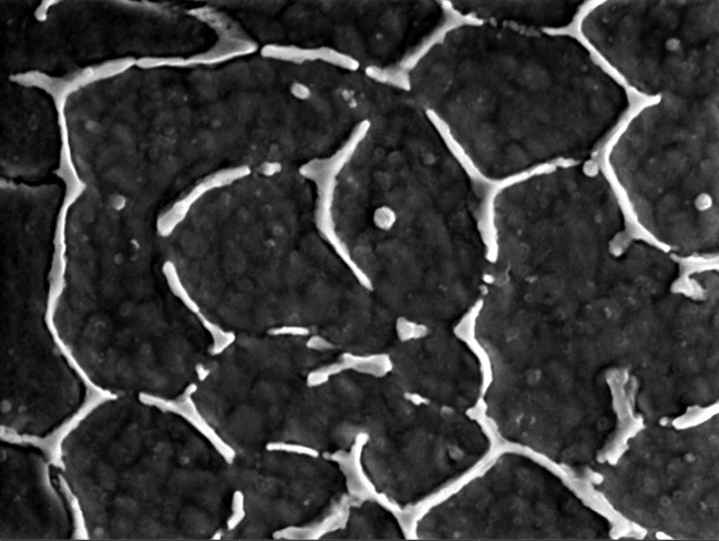
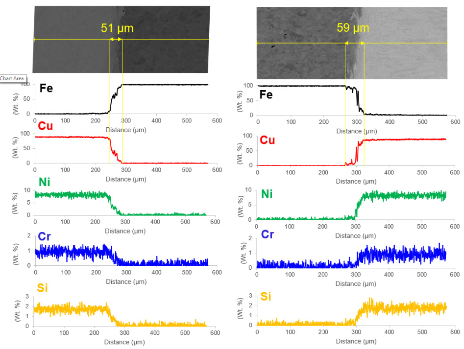
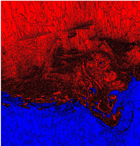
  • High-quality BSE contrast for phase discrimination

  • Low-kV imaging for detailed grain and substructure observation

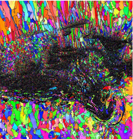
  • Full EBSD and EDS compatibility for multimodal studies

  • Automated panoramic imaging for weld zone evaluation


MIRA XR GM MONO Metal

Tescan Essence™ Image Snapper, Automated SEM Acquisition Tool

Unattended, large-area SEM imaging and stitching.

  • Produces seamless panoramic datasets from multiple fields

  • Ideal for weld inspection, defect observation, and interface mapping

  • Reduces operator time while improving reproducibility

GET IN Touch

Contact us

map

Where can you find us:

Tescan Brno
Libušina třída 21
623 00 Brno
Czech Republic

info@Tescan.com