WEBINAR | Up to 40% Faster Automated TEM Lamella Preparation with new Ga⁺ FIB Column

SEM Surface Analysis with Scanning Electron Microscopy  


Analyze surface and interface properties so you can better understand material performance. Tescan SEM solutions deliver precise SEM surface analysis across metals, polymers, ceramics, batteries, and geological samples. Examine morphology, grain structure, defects, and elemental composition to ensure reliable research and quality assurance.

SEM Surface Analysis

Contents

Hierarchical Study of Multi-Material Interfaces in Laser Powder Bed Fusion

Understanding material interfaces is critical in additive manufacturing, where mechanical properties depend on the bonding between dissimilar metals. High-resolution SEM analysis of the Cu7Ni2SiCr and Fe interface reveals grain alignment, microcracks, and diffusion zones that govern structural integrity.

  • Visualize microstructural gradients at multi-material boundaries

  • Detect defects and weak bonding zones at the interface

  • Correlate interface quality with mechanical performance


05_Phase map showing two separate phases
High-Resolution SEM Analysis of SBA-15-Type Mesoporous Silica Particles

Mesoporous silica (SBA-15 type) is widely used in catalysis and energy-related applications, where surface morphology and pore uniformity are essential. High-resolution SEM imaging provides nanoscale visualization of particle shape, pore arrangement, and surface roughness.

  • Examine ordered mesoporous structures with ultra-high-resolution SEM
  • Assess particle morphology for catalytic and adsorption efficiency
  • Identify defects or irregularities in pore distribution
06_Mesoporous Silica acquired at 500 eV with Axial detector-1
Electrospun Polymer Nanofibers: Properties, Applications, and Quality Assessment

Electrospun nanofibers require precise control of surface structure and fiber uniformity to ensure performance in medical and filtration applications. SEM imaging highlights fiber diameter, alignment, and surface smoothness for quality assessment.

  • Characterize nanofiber morphology at sub-micron scale

  • Detect irregularities such as beads or non-uniform thickness

  • Correlate fiber structure with application-specific properties
04_ Measurement of nanofiber diameters on homogeneous nanofibers after optimalization of process parameters-2
High-Temperature In Situ EBSD of Additively Manufactured Steel

Steel components fabricated by additive manufacturing undergo microstructural changes under thermal stress. Automated in situ EBSD at elevated temperatures reveals grain growth, recrystallization, and texture evolution in real time.

  • Monitor grain structure evolution during heating
  • Capture recrystallization and phase transformation pathways
  • Relate thermal behavior to mechanical reliability in service
01_Illustration of the comparison of results collected by automated in situ and ex situ experiments-3
SEM and EBSD Analysis After ECAP Processing of Aluminum

Equal-channel angular pressing (ECAP) refines aluminum grain structure for enhanced strength. SEM and EBSD analysis demonstrate grain refinement, boundary misorientations, and defect evolution introduced by severe plastic deformation.

  • Visualize ultrafine grain structures formed by ECAP
  • Quantify misorientation distributions with EBSD
  • Assess improvements in strength and ductility through microstructural control
01_Channeling contrast of the sample treated by 8 steps of ECAP-1
Ultra-High-Resolution Analysis of Fractured Ti-6Al-4V Alloy Surfaces

Fatigue failure is one of the most common failure modes in metals. It begins with small cracks or defects that gradually grow until they form a major fracture. High-resolution SEM imaging of fractured Ti-6Al-4V surfaces reveals striations, microvoids, and fracture origins that explain how these cracks evolve.

  • Examine nanoscale fracture features in titanium alloys
  • Identify initiation points of fatigue cracks
  • Link fracture morphology to and alloy performance
05_Dimples on the fractured surface-1
Enhanced Petrological Characterization with TESCAN Essence™ EDS

Complex geological samples often require both structural and compositional insight. TESCAN Essence™ EDS integrated within SEM imaging provides seamless mapping of mineral phases and trace element distributions.

  • Combine SEM morphology with EDS chemical analysis
  • Map elemental distributions across heterogeneous minerals
  • Improve workflow efficiency with integrated SEM–EDS characterization
02_Garnet porphyroblast distribution map of manganese revealing distinct zonation-1
High-Resolution Analysis of Battery Separators

Separator integrity is vital for battery safety and performance. SEM surface analysis uncovers pore morphology in separator membranes.

  • Visualize separator pore networks in high detail
  • Detect surface or structural defects that affect performance
  • Correlate microstructure with electrolyte uptake and safety
2_High-resolution SEM observation of polypropylene separator-1-1
Particle Size Characterization in Battery Powders

Powder morphology directly influences electrode packing density and electrochemical behavior. SEM imaging enables quantitative particle size analysis and surface defect detection in active battery materials.

  • Measure particle size distribution with high accuracy
  • Assess surface roughness and particle agglomeration
  • Correlate powder morphology with electrochemical performance

1_SEM examination of LiCoO2 particle properties-1

TESCAN Instruments & Technology

Used in This Workflow

Tescan VEGA Compact 

Tescan VEGA Compact is a versatile tungsten SEM designed for routine analysis. It combines reliable imaging, integrated microanalysis, and ease of use in a cost-efficient platform—ideal for everyday surface characterization tasks.

  • Daily materials analysis: Affordable tungsten SEM for routine surface studies
  • Integrated EDS: Faster imaging with seamless chemical microanalysis
  • High-vacuum performance: Delivers high-quality imaging and precise elemental analysis in full high-vacuum mode


VEGA Compact (3)

TESCAN VEGA

Tescan VEGA delivers robust performance for materials research, offering flexible imaging options and analytical capabilities. It is a reliable solution for laboratories that need a balance of imaging resolution, workflow efficiency, and affordability.

  • Robust analytical platform: Designed for a wide range of materials applications
  • Imaging and microanalysis integration: Ensures workflow efficiency
  • Reproducible results: Reliable data for research and quality assurance
VEGA LM Mat Science (1)

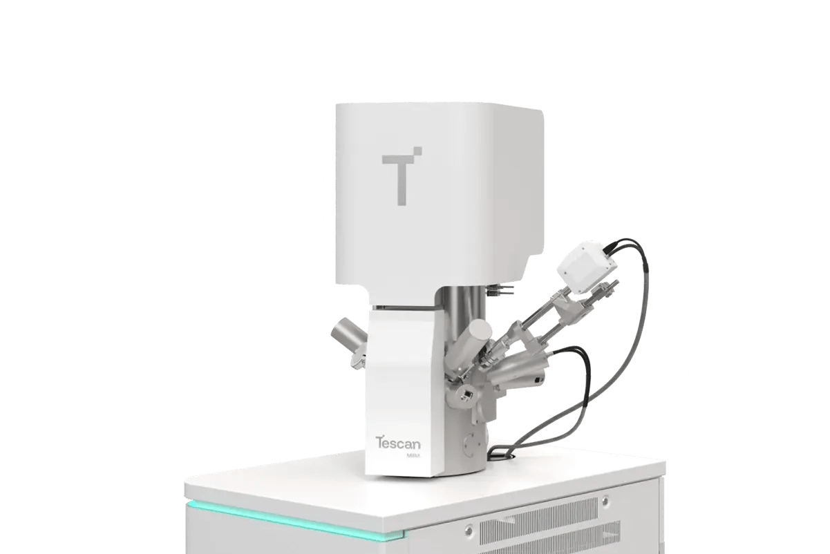
Tescan MIRA

Tescan MIRA is a high-resolution analytical FEG-SEM designed for materials characterization, research, and quality control. It delivers precise imaging and enables direct correlation of compositional data with SEM images for efficient surface and microstructural analysis.

  • Integrated Essence™ EDS: Acquire compositional data and overlay it directly onto SEM images
  • In-Flight™ Beam Tracing: Quickly set up beam parameters for optimal imaging and analytical conditions
  • Wide Field Optics™: Navigate easily and precisely across large or complex samples, even at low magnifications 
MIRA LM Mat Science

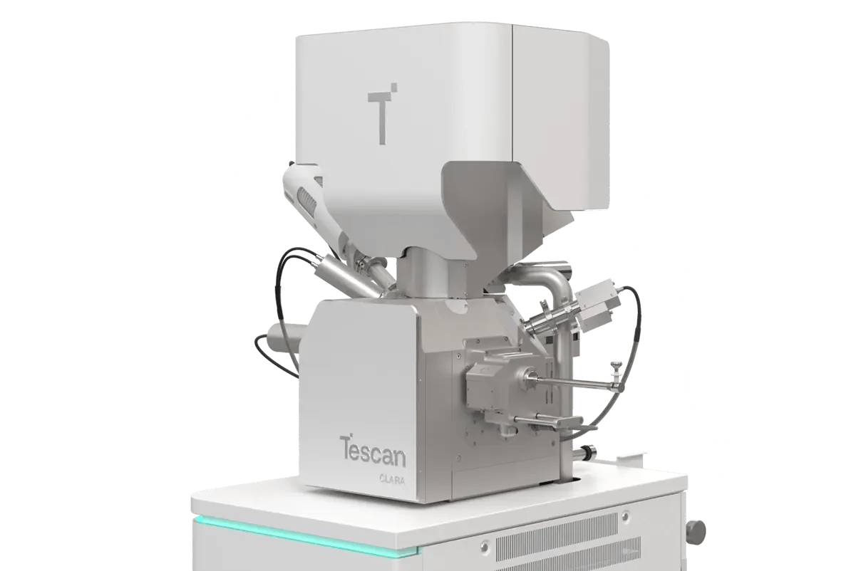
TESCAN CLARA

TESCAN CLARA™ is a field-free ultra-high-resolution SEM for imaging magnetic or beam-sensitive materials. Its selective BSE imaging, differentiated by take-off angle and energy, reveals hidden features and subtle material contrasts.

  • Selective BSE imaging: Dual in-column detectors with energy filtering for precise contrast
  • Field-free design: Ideal for magnetic and delicate samples
  • Low-voltage imaging: Clear surface detail with minimal beam energy
CLARA GM Mat. Science

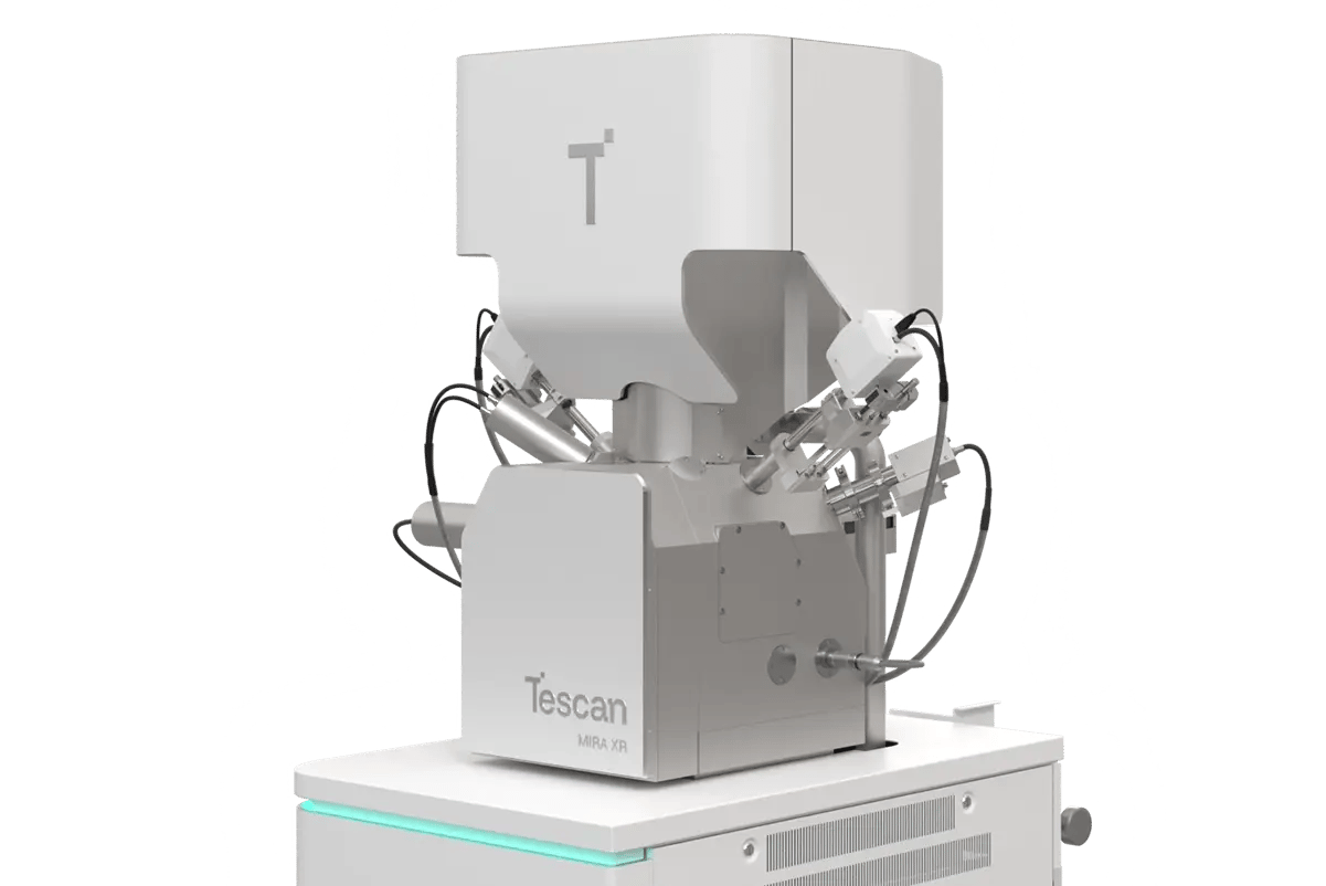
TESCAN MIRA XR

Tescan MIRA XR is an ultra-high-resolution SEM-EDS system for fast, precise materials analysis in research and quality control. It combines UHR imaging with automation to deliver reliable results and shorten time to data.

  • Dual Essence™ EDS: Simultaneous imaging and elemental analysis for rapid results
  • BrightBeam™ technology: High contrast and clarity at nano- and microscale
  • Wide Field Optics™: Quick navigation across large or complex samples
  • MultiVac™ mode: High-resolution imaging of sensitive samples without coating
  • In-Flight™ Automation: Automatic alignment and calibration for consistent imaging


MIRA XR GM MONO Metal

Sign up for a personal virtual demo

Our global team is available to answer questions about Tescan solutions for Material Science.

GET IN Touch

GET IN Touch

Contact us

map

Where can you find us:

Tescan
Libušina třída 21
623 00 Brno
Czech Republic

info@Tescan.com