WEBINAR | Dynamic-to-Detail Micro-CT in One Workflow: UniTOM HR 2

Structural and Chemical Analysis of Encapsulated Nanoparticles in Carbon Nanotubes

Multimodal 4D-STEM and EDX characterization of metal particles at the nanoscale.

Structural and Chemical Analysis of Encapsulated Nanoparticles in Carbon Nanotubes
Unlocked content

Investigating Structure–Function Relationships of Nanomaterials

Using Tescan TENSOR’s multimodal capabilities, this study demonstrates how to perform full analytical STEM characterization of materials using the conventional STEM imaging and EDX mapping complemented with advanced 4D-STEM structural analysis. The results obtained from individual metal nanoparticles that were encapsulated within multi-walled carbon nanotubes provide a detailed view of particle composition, crystallinity, and grain orientation, resolved at the nanometer scale and acquired within a single integrated workflow from a large region of interest.

Why Characterize Encapsulated Nanoparticles

with 4D-STEM?

01
Root of the Problem

Efficient Process Development of New Materials Requires Nanoscale Mapping of the Morphology, Chemistry, and Crystallinity at the Same Time

The internal structure of metal nanoparticles can be influenced by the preparation process, as well as their spatial surrounding, for example when grown in narrow carbon nanotubes. However, the large difference in the atomic number of carbon and small metal nanoparticles present difficulties for standard electron microscopy techniques.

To study the spatial relationship between a host nanotube and its encapsulated particles, a multimodal approach combining compositional mapping with orientation-sensitive diffraction is necessary.

02
Materials and Methods

Correlative STEM Imaging, EDX Mapping, and 4D-STEM Analysis

Carbon nanotubes containing iron nanoparticles were analyzed using a multimodal workflow on the Tescan TENSOR platform. STEM imaging was used for morphology visualization, EDX mapping for elemental composition, and 4D-STEM for orientation analysis. The setup enabled each technique to target the same region under optimized conditions. STEM imaging used a 6.5 mrad convergence semiangle and 100 pA probe current, while EDX mapping was performed with a higher probe current (10 nA) and ~1 nm probe diameter over a 600 s acquisition.

For crystallographic analysis, 4D-STEM orientation mapping was conducted using a 2 mrad convergence semiangle, 250 pA probe current, 2.5 nm pixel size, and 2 ms dwell time. Templates of diffraction patterns were derived from kinematic CIF models of metallic iron. High resolution STEM imaging was done at a 10 mrad convergence semiangle and 65 pA current, allowed wall layer spacing to be measured via image FFTs. All techniques were spatially correlated using the same acquisition platform.

03
Results and Discussion

Specific Mechanism of Nanoparticles Growth in Carbon Nanotubes Revealed

STEM imaging showed growth of 20-nm particles inside carbon nanotubes, which were fully enclosed within the nanotube walls, without external aggregation or attachment. EDX mapping confirmed that the  nanoparticles were made primarilly of iron, with no elemental diffusion into the carbon matrix. High resolution STEM imaging revealed consistent graphitic interlayer spacing around 0.34 nm, while wall thickness varied from 5 to over 15 layers across different nanotubes.

Phase and orientation analysis revealed both aligned and misaligned grains relative to the carbon shell, indicating that the confinement in the nanotubes could have guided crystal growth. The nanobeam diffraction analysis enabled region-specific orientation mapping (4D-STEM) that decoupled particle structure from the surrounding carbon walls. Together, the integrated dataset provided a detailed view of particle identity, placement, and orientation within the carbon nanotube confinement.

GET IN Touch

Contact us

Get the most out of Tescan

This is more than information; it's an advantage. We've compiled our technical whitepapers, detailed product flyers, and on-demand webinars to provide you with the knowledge that makes a real difference. Sign up now to access the insights you need to make an impact.

Tescan Instruments & Technology

Used in This Workflow

Tescan TENSOR

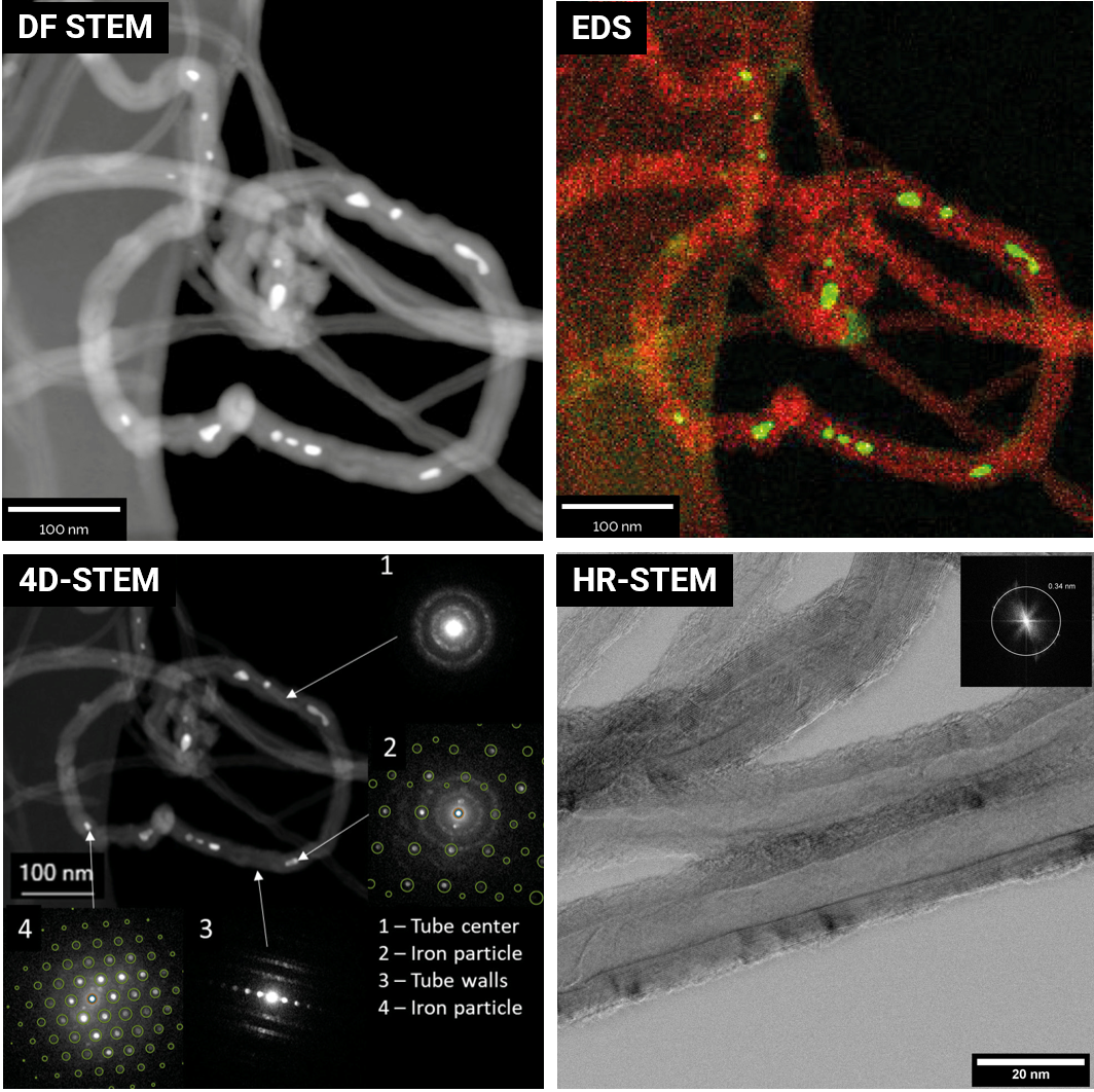
A fully integrated analytical scanning transmission electron microscope that captures imaging, diffraction, and elemental data simultaneously for multimodal nanoscale characterization.


  • 4D-STEM for crystallographic orientation and phase mapping

  • Large solid-angle EDX detectors and 100 kV electron acceleration providing clearer and unambiguous data for efficient nanoscale chemical analysis

  • Precession-assisted nanobeam diffraction for high-quality indexing of acquired diffraction patterns
TENSOR_1

GET IN Touch

with specialist

map

Where can you find us: 

Tescan
Libušina třída 21
623 00 Brno
Czech Republic

130405923 us US 37.09024 -95.712891 25.3575 29.349345 20.67957527 42.082797 39.91384763 -33.693421 13.93320106 3.039986586 31.997988 38.050985 47.579533 48.1485965 58.375799 54.663142 19.195447 56.975106 50.493053 45.868592 10.79556993 44.35660598 43.2371604 55.536415 14.557577179752773 32.100937 -6.116829 -6.212299277967318 23.7104 -33.471062 31.998740087 -23.69149395 43.462349 51.529848 49.1893523 49.197486 25.072375 31.075811 1.299027 40.676979 52.30150662 51.013813 35.684121 37.479653 52.246622 40.581349 39.911632 -26.1811371 41.818215 33.429928 -12.08688

No distributors found.