WEBINAR | Up to 40% Faster Automated TEM Lamella Preparation with new Ga⁺ FIB Column

Phase and Orientation Analysis of Cu-Rich Sulfide Ceramics Using 3D ED and 4D-STEM on a Single Lamella

This workflow combines 3D electron diffraction and 4D-STEM to identify and validate a secondary phase in thermoelectric Cu-rich sulfide ceramics — all from the same sample lamella.

hero
hero
Unlocked content

From Structure Determination to Spatial Mapping — an All-in-One Workflow

Polycrystalline thermoelectric materials often exhibit complex nanoscale phase distributions and crystal orientations, factors that directly influence their transport properties. Yet most characterization methods capture either structure or spatial context, not both. Adding to the challenge, each technique typically requires a separate sample form.

Tescan TENSOR solves this with an integrated multimodal workflow that combines electron diffraction tomography (3D ED) and precession-assisted 4D-STEM — performed on the same FIB-prepared lamella. No additional sample prep. No instrument handoff.

In this study of Cu₂.₃Mn₀.₇GeS₄ ceramics, researchers identified and validated the crystal structure of a secondary phase, then mapped its spatial distribution and orientation. This is all within a single, uninterrupted session.

Why Combine 3D ED

and 4D-STEM?

01
Root of the Problem

Complex Phase Distributions in Thermoelectrics

Thermoelectric sulfides like Cu₂.₃Mn₀.₇GeS₄ often contain multiple coexisting phases — such as stannite (tetragonal) and enargite (orthorhombic) — with similar structures that make them difficult to distinguish. These materials are further challenged by faults, disorder, and grain-level variation introduced during synthesis.

Traditional techniques like EDX mapping and TEM/STEM imaging lack the sensitivity and crystallographic resolution to distinguish the fine structural differences of different structural phases.

Tescan TENSOR enables a unique combination of 3D electron diffraction tomography (3D ED) and 4D-STEM, allowing researchers to solve atomic structures from individual grains within a single lamella of a polycrystalline sample. The same lamella can then be used for regular 4D-STEM nanoscale mapping of the distribution and transitions of different phases within the studied material.

02
Materials and Methods

Structure determination and phase mapping from the same lamella

A Cu₂.₃Mn₀.₇GeS₄ sample was prepared by mechanical alloying and DC pulsed sintering at 873 K. A region with distinct grains was thinned via FIB for lamella-based analysis.

One ~200 nm grain was examined by 3DED using 1.1° precession over a ±45° tilt range in 1° steps. The resulting 3D diffraction dataset was processed in PETS and JANA software packages, yielding a previously unconfirmed enargite-type structure. A crystallographic file (CIF) was generated for 4D-STEM mapping and phase distribution analysis.

Following 3D-ED structure determination of the enargite phase, 4D-STEM mapping was performed using 14 mrad precession and 2 mrad beam convergence semi-angle in a 720 × 900 nm region on the same lamella. Diffraction templates generated from both stannite (published cif file) and enargite (derived from 3D ED) phases were used to determine the phase and orientation maps in TENSOR’s Explore software. 

03
Results and Discussion

Structural Domains and Phase Interfaces

3D ED confirmed the presence of an orthorhombic enargite-type phase in Cu₂.₃Mn₀.₇GeS₄, providing a unique structural solution for subsequent mapping. The obtained CIF file and subsequently generated diffraction templates enabled precise assessment of phase distribution across the broader sample.

4D-STEM mapping revealed a mosaic of stannite and enargite grains with sharp phase boundaries. Dislocations and stacking faults frequently coincided with these interfaces, suggesting a structural link between defect formation and phase transitions during sintering.

Orientation maps showed domain alignment within individual grains, disrupted by localized misorientations at phase junctions. The combined 3D ED and 4D-STEM approach provided a full crystallographic picture, linking unit-cell-level structure to mesoscale grain behavior and offering insight into structure–property relationships in thermoelectric materials.

GET IN Touch

Contact us

Get the most out of Tescan

This is more than information; it's an advantage. We've compiled our technical whitepapers, detailed product flyers, and on-demand webinars to provide you with the knowledge that makes a real difference. Sign up now to access the insights you need to make an impact.

Tescan Instruments & Technology

Used in This Workflow

Tescan TENSOR™ – Precession-Assisted 4D STEM Platform

A fully integrated, multimodal, analytical STEM microscope combining high-speed diffraction imaging, orientation mapping, and automated precession workflows.

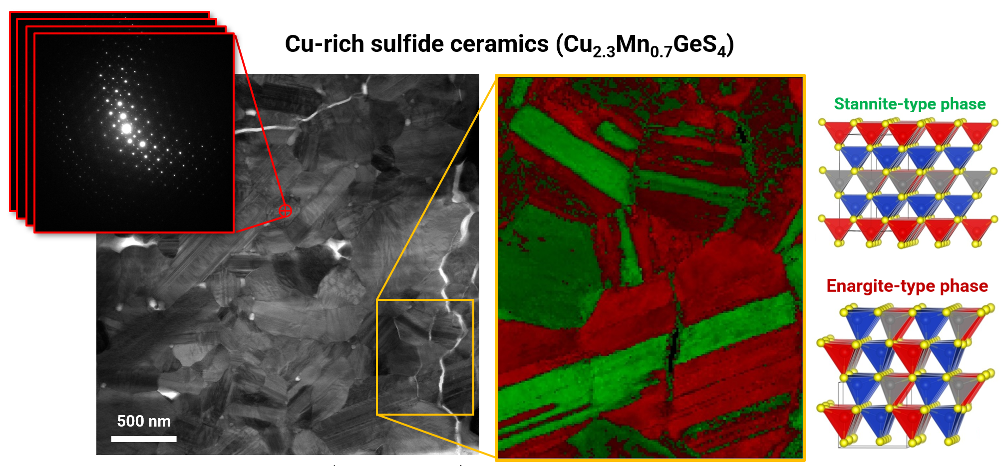
  • Enables 3D ED data acquisition with 4D-STEM mapping, from the same lamella

  • Automated beam control and precession alignment for repeatable measurements

  • Real-time phase and orientation mapping with Explore software
TENSOR_1

GET IN Touch

Contact us

map

Where can you find us:

Tescan Brno
Libušina třída 21
623 00 Brno
Czech Republic

info@Tescan.com