Deliver High-Precision TEM Lamella Preparation in Semiconductors   


Prepare uniform, damage-free lamella with workflows that preserve structure and ensure consistent results from 7 nm to 66 nm nodes.

TEM_Lamella_Preparation

Tescan solutions

for advanced research in semiconductors
Gas-assisted delayering and TEM lamella preparation from a 7nm chip

Combine gas-assisted delayering with inverted geometry and precise endpoint control to prepare sub-20 nm TEM lamella from 7 nm devices. This integrated workflow preserves structural integrity and delivers reliable high-resolution analysis.

  • Nanoflat chemistry: Maintains planarity and contrast across complex multilayer stacks
  • Inverted geometry: Improves lamella stability, reduces curtaining, and enables precise thinning
  • Real-time inspection: Preserves delicate transistor and contact features for accurate TEM imaging 
4_Inverted TEM lamellae prepared from 7nm FinFET device_1x
TEM sample preparation from a 10nm FinFET device

Prepare sub-10 nm TEM lamella from FinFET gate and fin regions with a workflow that combines precise targeting, stable in-situ lift-out, inverted geometry, and low-energy polishing. Structural detail is preserved for accurate, consistent high-resolution analysis. 

  • Inverted geometry: Improves mechanical stability and reduces curtaining during thinning
  • Low-energy polishing: Removes damage layers while maintaining crystalline and interface clarity
  • Site-specific preparation: Delivers consistent, high-quality lamella from both gate-cut and fin-cut regions
3_200 kV TEM image of Fin-cut geometry TEM sample_1x
TEM Specimen Preparation from a 66 nm SDRAM Sample

Produce Ga-free TEM lamella from SDRAM devices with a workflow that combines controlled thinning and real-time inspection. This process minimizes damage, preserves interface integrity, and delivers electron-transparent samples for accurate high-resolution analysis.

  • Inert ion milling: Avoids gallium contamination and protects native material chemistry

  • Low-energy thinning: Minimizes amorphous damage and maintains interface clarity

  • Real-time inspection: Ensures uniform thickness and stable lamella for reliable TEM or STEM imaging 
4_Electron transparent sample made from DRAM_1x-1

Tescan Solutions

for TEM Lamella Preparation in Semiconductors

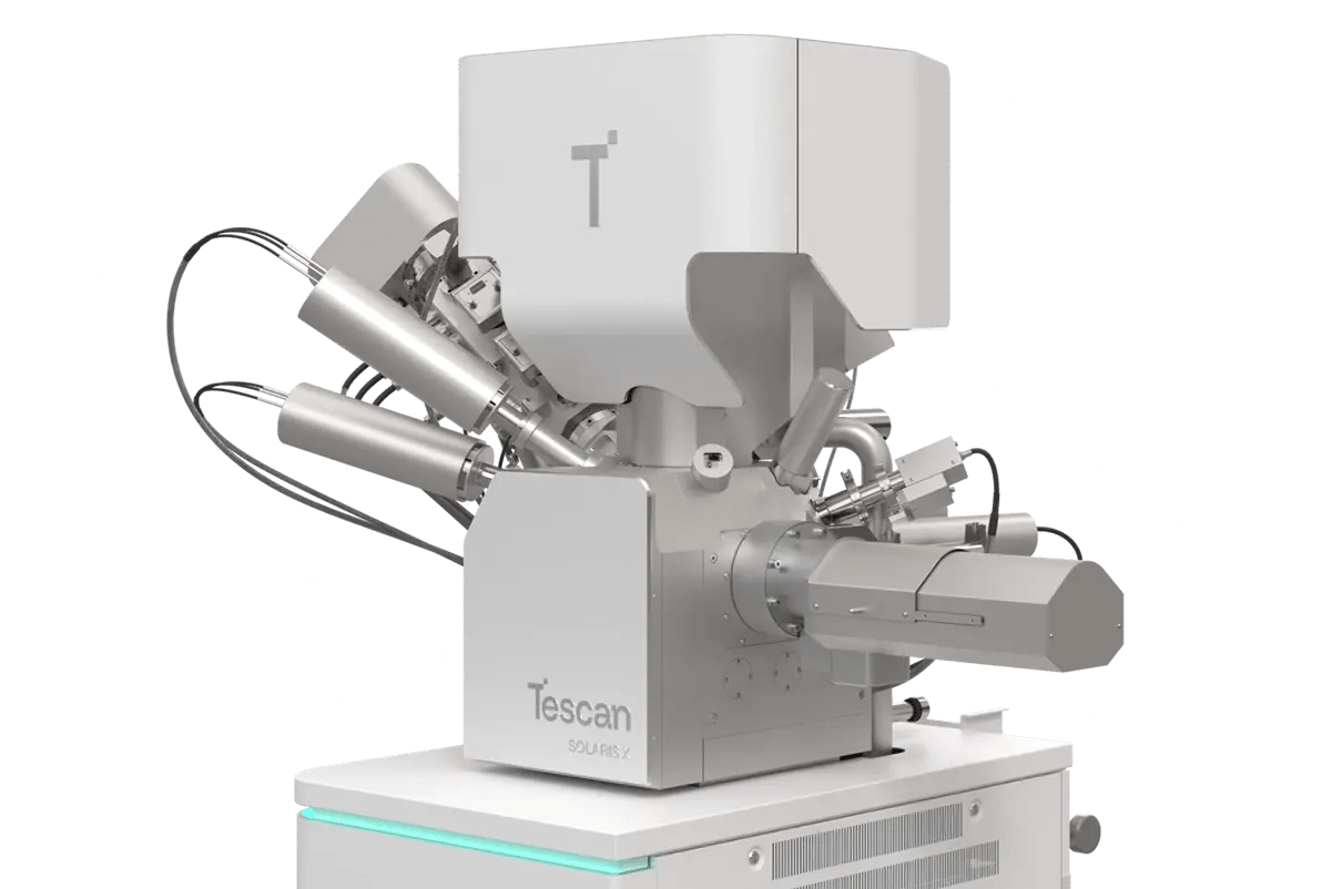
Tescan SOLARIS X FIB-SEM

Tescan SOLARIS X FIB-SEM delivers the precision, control, and integration required for preparing sub-20 nm TEM lamella from 7nm node devices. The Xe⁺ plasma-based system combines gas-assisted delayering, trenching, and thinning within a single, in-situ workflow—eliminating air exposure and reducing variability. OptiLift™ nanomanipulation supports stable lamella handling, while low-keV final polishing ensures structural integrity for high-resolution imaging.

  • Integrated Xe⁺ plasma FIB-SEM platform: Complete TEM preparation without transferring between systems

  • Gas-assisted delayering: Remove layers from M10 to contact with control and repeatability

  • In-situ lift-out with OptiLift™: Reduce mechanical stress and contamination during lamella transfer

  • Sub-20 nm lamella preparation: Achieve transistor-level resolution suitable for HR-TEM or STEM

  • Inverted geometry and 1 keV final thinning: Minimize curtaining and preserve structural integrity across layers
SOLARIS-X2

Tescan SOLARIS X with iFIB+™  

Tescan SOLARIS X with iFIB+™ combines fast bulk milling and precise low-current thinning to deliver clean, accurately targeted TEM lamella for advanced semiconductor failure analysis.

Its inert Xe ion source prevents chemical artifacts and contamination common with gallium FIB, while integrated SEM imaging supports real-time monitoring and inspection. This ensures lamella are prepared with the optimal thickness and preserved structure for downstream STEM and EDS workflows.

  • iFIB+™ Xe plasma column: Supports both high-current bulk milling and delicate lamella thinning
  • Inert ion beam: Avoids chemical artifacts and eliminates gallium implantation
  • Final thinning below 5 keV: Minimizes amorphous damage at critical interfaces
  • Real-time SEM imaging: Enables quality control before lift-out
  • Wide beam current range: Provides both speed and precision in a single system
SOLARIS-X2

Triglav™ SEM Column

The Triglav™ SEM column provides stable, high-resolution imaging at low keV, crucial for precise end-pointing during TEM lamella thinning. Low landing energy operation reduces charging and beam damage, enabling detailed imaging of buried FinFET features throughout the thinning process.

  • High-resolution low-keV imaging: enables precise end-pointing down to gate and fin interfaces
  • 2 keV in-beam SE detection: delivers clear surface contrast with minimal beam-induced damage
  • Stable column alignment: ensures consistent image quality across different magnifications and depths
  • Accurate SEM-FIB registration: supports precise trenching and lamella targeting

Orage™ Ga FIB Column 

The Orage™ Ga FIB column gives you precise control across the full voltage range, making it well-suited for complex lamella preparation. With stable beam performance at low energies, you can perform final polishing at 1 keV to remove amorphous layers and preserve key interfaces. This is essential for accurate TEM analysis of 10 nm FinFET devices.

  • High-resolution ion beam control: lets you trench and thin from bulk material down to sub-10 nm with confidence

  • 1 keV final polish: helps you remove surface damage while maintaining crystalline detail

  • Low-voltage performance: allows you to reduce amorphization and expose clean material interfaces

  • Optimized for inverted geometry: gives you consistent thinning and lamella stability throughout final prep

Sign up for a personal virtual demo

Our global team is available to answer questions about Tescan solutions for Semiconductors.

GET IN Touch

Contact us

map

Where can you find us:

Tescan Brno
Libušina třída 21
623 00 Brno
Czech Republic

info@Tescan.com