1. Root of the Problem
Why Standard TEM Prep Workflows Fall Short on 10 nm FinFET Devices
Preparing high-quality TEM lamella from 10 nm FinFET structures demands extreme precision. Yet standard FIB-SEM workflows often struggle to meet these requirements. Thinning below 10 nm without damaging gate or fin features is technically challenging, especially when sample handling, beam damage, or curtaining disrupt the process.
FinFET gate and fin structures are small, buried, and geometrically complex. Even minor misalignment during trenching or lift-out can obscure critical interfaces or cause lamella distortion. And final thinning steps often introduce amorphization that degrades TEM resolution.
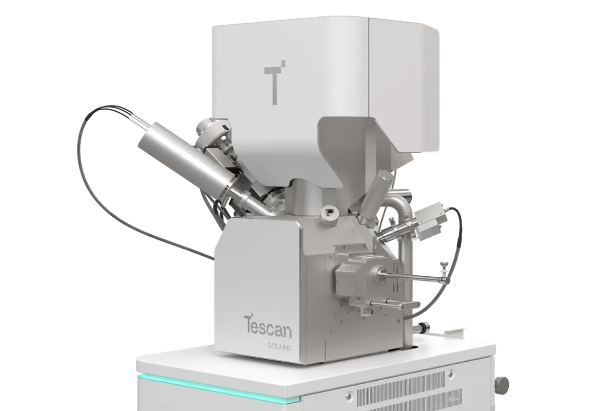
TESCAN SOLARIS addresses these challenges with a finely tuned, application-focused approach to TEM sample prep.
- In-situ lift-out minimizes contamination and mechanical stress
- Inverted geometry supports lamella stability during thinning
- SEM end-pointing enables accurate targeting of gate and fin regions
- 1 keV final FIB polish removes damage layers while preserving structure
- Reliable results across both gate-cut and fin-cut configurations
Extracting sub-10 nm lamella from FinFET devices no longer needs to be a bottleneck. With SOLARIS, you gain a reliable, repeatable path to clean, TEM-ready samples.
2. Materials and Methods
How TEM Lamella Were Prepared from FinFET Devices Using TESCAN SOLARIS FIB-SEM
A 10 nm FinFET device was selected to demonstrate routine TEM lamella preparation. The region of interest was located using high-resolution SEM imaging with a 2 keV in-beam secondary electron detector to ensure accurate targeting of gate and fin structures.
Trench milling and sample thinning were performed using the Orage™ Ga FIB column, with Pt protection deposited before lift-out. The lamella was extracted in-situ using a nanomanipulator and attached directly to a TEM grid for final thinning.
An inverted geometry was used to improve mechanical stability and minimize curtaining during polishing. Final FIB cleaning at 1 keV ensured sub-10 nm lamella thickness while preserving structural integrity at material interfaces.
This workflow enabled reliable preparation of both gate-cut and fin-cut samples, suitable for high-resolution cross-sectional TEM analysis without structural distortion or contamination.
3. Results and Discussion
High-Resolution TEM Analysis of Gate and Fin Structures in FinFET Devices
TESCAN SOLARIS FIB-SEM enabled consistent preparation of sub-10 nm lamella from both gate-cut and fin-cut regions of a 10 nm FinFET device. Inverted geometry combined with low-keV polishing preserved the structural integrity of metal, dielectric, and semiconductor layers across the lamella.
TEM imaging revealed crisp interfaces and minimal amorphous damage, allowing for clear visualization of gate architecture, fin contours, and interconnect structures. The quality of thinning enabled analysis of critical features such as contact spacing, channel uniformity, and interface quality.
Gate regions displayed well-preserved poly-Si and high-k stack structures, while fin-cut lamella provided high-contrast views of fin pitch, oxide boundaries, and diffusion layers. Cross-sectional images confirmed uniform lamella thickness and precise feature retention across samples.
This workflow proved to be a reliable path for device-level failure analysis, structural validation, and process insight at the 10 nm technology node. It delivered the precision and consistency engineers need to push semiconductor development forward with confidence.