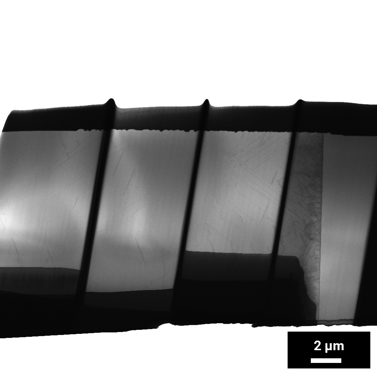
%20lamella%20prepared%20in%20trench%20after%20undercut.png?hsLang=en)
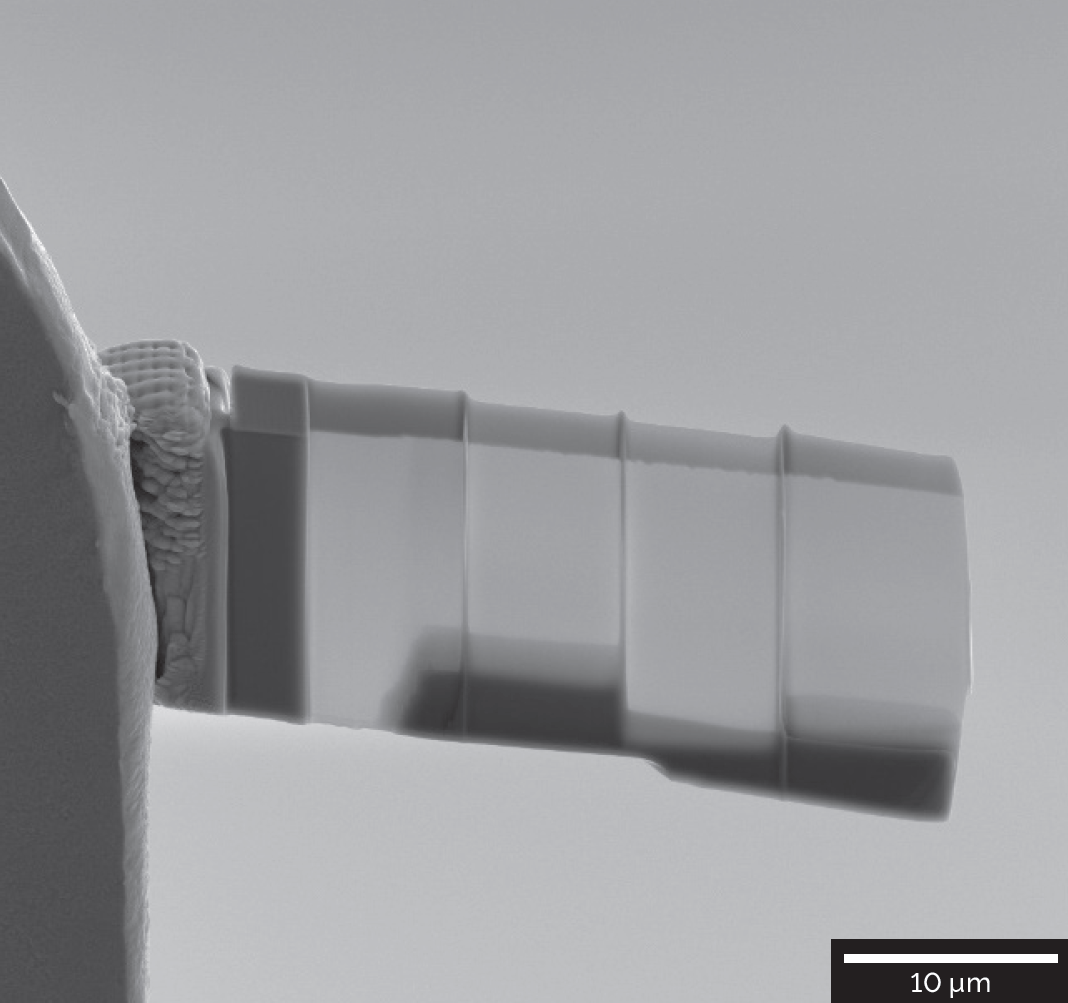
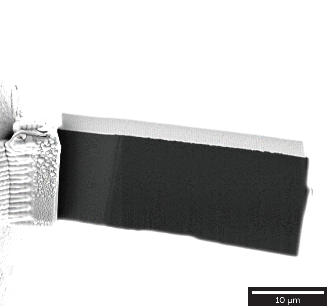
Tescan OptiLift™
Tescan OptiLift™ is a unique nanomanipulator system designed for maximum flexibility during TEM lamella preparation. Its ability to operate below the ion column allows full 360° rotation and precise angle adjustment of specimens after lift-out.
- 360° rotation: Freedom to optimize geometry for thinning and polishing
- Below-column positioning: Greater working space and improved sample handling
- Precise alignment: Ensures uniform lamella preparation even in large or complex specimens
- Reliable lift-out: Enables preparation of lamellae up to 55 × 30 µm without distortion